High Quality Low Cost

Printed Circuit Boards

Click here for instant quote

If you prefer to send us your files for a quote, or if you have manufacturing questions, please call us toll free at 800.791.5370 or contact us. We will be glad to help!

IPC Logo
ISO 9001 Logo
UL Logo
ROHS Logo
Conflict Free Minerals Logo
Reach Logo

PCB Capabilities

Rigid PCB capabilities

  • Up to 42 layers
  • FR4, Aluminum, Rogers, Nelco and more
  • Controlled Impedance
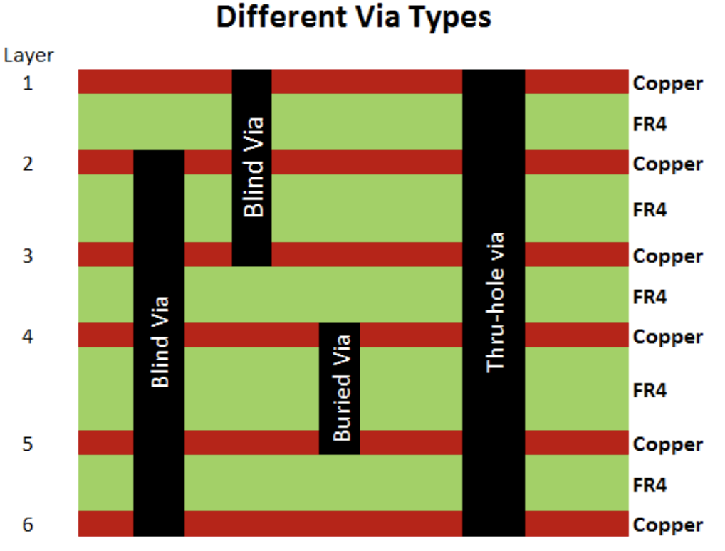
  • Blind & Buried Vias (HDI)
  • Via In Pad / Active Pad
  • Class II & Class III
  • ISO 9001:2015
  • RoHS and REACH Compliant
Learn more
Assembly Capabilities

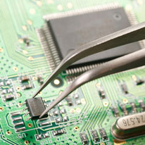
PCB Assembly Services

  • Fast Turn Times
  • Turnkey/Kitted/Consigned
  • Surface Mount (SMT) / Thru hole
  • Single- or Double-sided Placement
  • Lead or Lead-free
  • BGA
  • Fine Pitch
  • X-Ray
  • Functional Testing
Learn more
Other Services

Other Services

  • Flex
  • Rigid-Flex
  • Stencils
  • Cables
  • Full Box Builds
  • Engineering Services
Learn more

PRIME PROTOTYPE SPECIAL PRICING

No hidden fees

-----divider----

Our prototype special pricing is perfect for hobbyists, students or multi-million dollar corporations looking to get a quick and simple prototype to prove their design before committing to a larger and more expensive order. Please read the details on what specifications are offered under this discounted program. If you need different specifications than what is offered, click here for a full-spec quote or contact us.


  • 2 Layer
  • $ 29
    each, Qty 4
  • 6 Day Lead Time
  • $116 Total
  • Buy Now
  • 4 Layer
  • $ 54
    each, Qty 4
  • 7 Day Lead Time
  • $216 Total
  • Buy Now
  • 6 layer
  • $ 89
    each, Qty 4
  • 10 Day Lead Time
  • $356 Total
  • Buy Now
  • 8 Layer
  • $ 109
    each, Qty 4
  • 11 Day Lead Time
  • $436 Total
  • Buy Now

PRIME Solutions

We are committed to the continuous improvement of our services to our customers

-----divider----

Order with confidence; we stand behind our products and services. We will do everything we can to be sure you are completely satisfied with your order.

Easy Quote Icon

Easy Quote Form

We continually look for ways to streamline and improve our online quote process so you can be confident your online quotes are accurate with no surprises after your order is placed.

Instant Price Icon

Instant Pricing

Our online quote form is available to you any time, day or night. Coming soon as Assembly and Stencil quoting capabilities.

Testing Icon

No Tooling or Test Charges

We never charge tooling so you can change revs as often as you need. We electrically test all our boards at no additional cost to you.

No Hidden Fees Icon

No Hidden Fees

Tired of 'handling fees...', whatever those are? We never charge additional fees. Your online quote is the total cost of your order plus the shipping method of your choice.

Proto and Production Icon

Proto and Production

We process all size orders from 1 piece to 1,000,000 pieces. We can handle your proto and full scale production needs.

Fast Lead Times

Fast Lead Times

Need boards in a hurry? We've got you covered. Depending on the size and specs of your order, we can ship in as little as 2 business days and be on your doorstep the 3rd day.

World Class Quality Icon

World Class Quality

Our manufacturing partners are some of the best in the world. We can build just about any design you can dream up; we've seen it all.

ISO and UL Certified PCBs Icon

ISO and UL Certified PCBs

All of our manufacturing partners are at a minimum ISO 9001:2015 and UL certified.
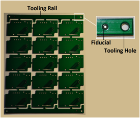
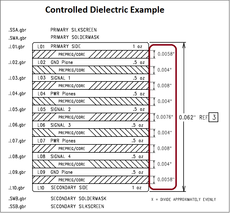
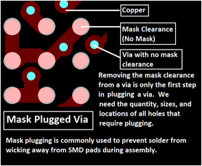
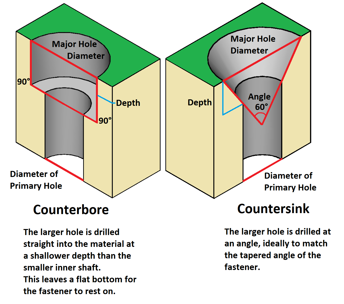
PCB Tips

Helpful tips for your next project

-----divider----

New tips added all the time, check back occasionally to see what's new.

Array Design Tips

The primary reason for having your boards delivered in an array is to make automated assembly faster and less expensive. Running an array of boards through a pick-and-place machine is far more efficient than sending them through one at a time.

Tech Tip Image One
Controlled Dielectric or Controlled Impedance?

What is the difference between Controlled Dielectric and Controlled Impedance regarding PCB fabrication? The purpose of controlling dielectric or impedance is essentially the same, to achieve a target impedance on one or more signal lines on a printed circuit board.

Tech Tip Image One
Via Tenting, Plugging, and Filling

There are many reasons a printed circuit board designer might want to have a via tented, plugged or filled. First, let's start with defining these terms since they can be frequently misused and misunderstood.

Tech Tip Image One
Countersink vs. Counterbore

A countersink is a cone shaped hole cut into the laminate. It is typically used to allow the tapered head of a screw to sit flush with the top of the laminate. By comparison, a counterbore makes a flat-bottomed hole and its sides are drilled straight.

Tech Tip Image One
Solder Mask

Solder Mask is a protective coating applied to the bare printed circuit board. Bare boards are covered with mask to prevent accidental solder bridging during assembly and to help protect the board from the environment.

Tech Tip Image One
Copper Thickness

The most common unit of measure for the copper thickness on a printed circuit board is ounces (oz). But how thick is that? It's the resulting thickness when 1 oz of copper is pressed flat and spread evenly over a one square foot area.

Tech Tip Image One
Dielectric Stacks

Standard Dielectric Stack diagrams for 4- to 10-layer boards from .8mm to 3.2mm

Tech Tip Image One
Drilling and Drill File

Essentially they are the same thing and many engineers use the terms interchangeably. Technically, the term "via" should be used when the hole is used to pass signal to another layer of your board and not for mounting a thru-hole component.

Tech Tip Image One
Final Finish Comparison

There are many factors to consider when selecting a final finish for your printed circuit board. Below is a consolidated list of popular finishes and their general characteristics.

Tech Tip Image One
PCB CAM Tooling Guidelines

When we receive artwork for a printed circuit board, many things are checked and adjusted to ensure the board is fabricated as closely as possible to the original design. If we notice something that appears unusual, we'll hold the order and question the designer's intent.

Tech Tip Image One
Rigid Specifications

We don't need much information to manufacture a bare printed circuit board. Often, all we receive are the digital Gerber files showing the copper layers, solder mask, silk screen and a drill file.

Tech Tip Image One
Accepted File Formats

At PCB Prime, we can accept a variety of file formats to manufacture or assemble your printed circuit board. A list of accepted formats is listed below.

Tech Tip Image One
Array Design Tips
Controlled Dielectric or Controlled Impedance?
Via Tenting, Plugging, and Filling
Countersink vs. Counterbore
Solder Mask
Copper Thickness
Dielectric Stacks
Drilling and Drill File
Final Finish Comparison
PCB CAM Tooling Guidelines
Rigid Specifications
Accepted File Formats