PCB-TIPS
Accepted File Formats
Array Design
CAM Tooling Guidelines
Controlled Dielectric or Controlled Impedance?
Countersink vs Counterbore
Default Rigid PCB Specs
Dielectric Stacks
Drilling and Drill File
Fabrication Drawing/Fab Print
Final Finish Comparison
How Thick Is 1oz Copper?
How to Avoid Engineering CAM Hold
Minimizing Bow and Twist
Solder Mask
Via Tenting, Plugging, and Filling
What is Copper Thieving?
Accepted File Formats
At PCB Prime, we can accept a variety of file formats to manufacture or assemble your printed circuit board. A list of accepted formats is listed below. Click the link to take you to a more in-depth explanation of each option. We'll be glad to answer any questions regarding the accepted file types or review the files you have if you aren't sure.
TIP: To ensure nothing is lost, please .zip all relevant files into a single .zip or .rar file.
Bare PCB fabrication
PCB Assembly (PCBA)
In order to assemble a PCB, we need the same files that are needed to fabricate the bare board (see above), plus information regarding what components will be placed on your board and where. The following files are needed.
- BOM (Bill Of Materials)
- XYRS / Pick and Place (PNP) / Component Placement List (CPL)
- Solder Paste (for Stencil)
- Photos of a correctly assembled board (top and bottom, if available but not required)
- Any Special Instructions (if applicable)
Stencils
To manufacture a stencil, we will need the paste layers for your array in Gerber format, preferably RS-274X format. We will send you a check plot so you can confirm everything looks correct before we start your order.
Gerber RS-274X
This is the most current Gerber format and is widely viewed as the accepted industry standard. All modern PCB layout tools will output in this format, older tools may be limited to the obsolete 274D format. 274X (extended) format is preferred since the aperture definitions for interpreting the width, size and shape of the features are embedded within each file as opposed to the original Gerber RS-274D format which relies on generating a separate aperture list for each file. Click here to see an example of an aperture file.
TIP: When submitting files in either Gerber format, we also need a CNC Drill file (see below). Depending on your layout software, this may automatically output when exporting your Gerber data, some software packages require this to be exported as a separate step.
TIP: Be careful not to use free layout software distributed by PCB fab (fabrication) shops since they will NOT output Gerber format, you'll be locked into using their service to manufacture your boards.
When outputting RS-274X Gerber format, there will be a separate file generated for each "layer" of your circuit board. An important point to understand is there are two different ways the word "layer" is used in the industry. When discussing the different files that comprise your PCB, each file is considered a layer. Top solder mask layer, top copper layer, top silk screen layer, CNC drill file, etc.
When discussing the specifications of your design on a technical level and for costing purposes, the number of layers refers to how many copper layers your design has. A "4 Layer" board can consist of many different Gerber, drill and fabrication files but in this sense, only contains 4 different layers that contain copper.
TIP: After exporting your Gerber and CNC Drill files, zip them together into a single zip file. We can also accept .rar compressed files. Add any fabrication notes or pictures to the zip that need to be included. Any of these standard formats are acceptable. TXT, PDF, DOC, DOCX, XLS, XLSX, CSV, PPT, PNG, JPG, DWG, etc.
By zipping your files into a single zip, this eliminates the chance that one or more of your files to become separated and lost.
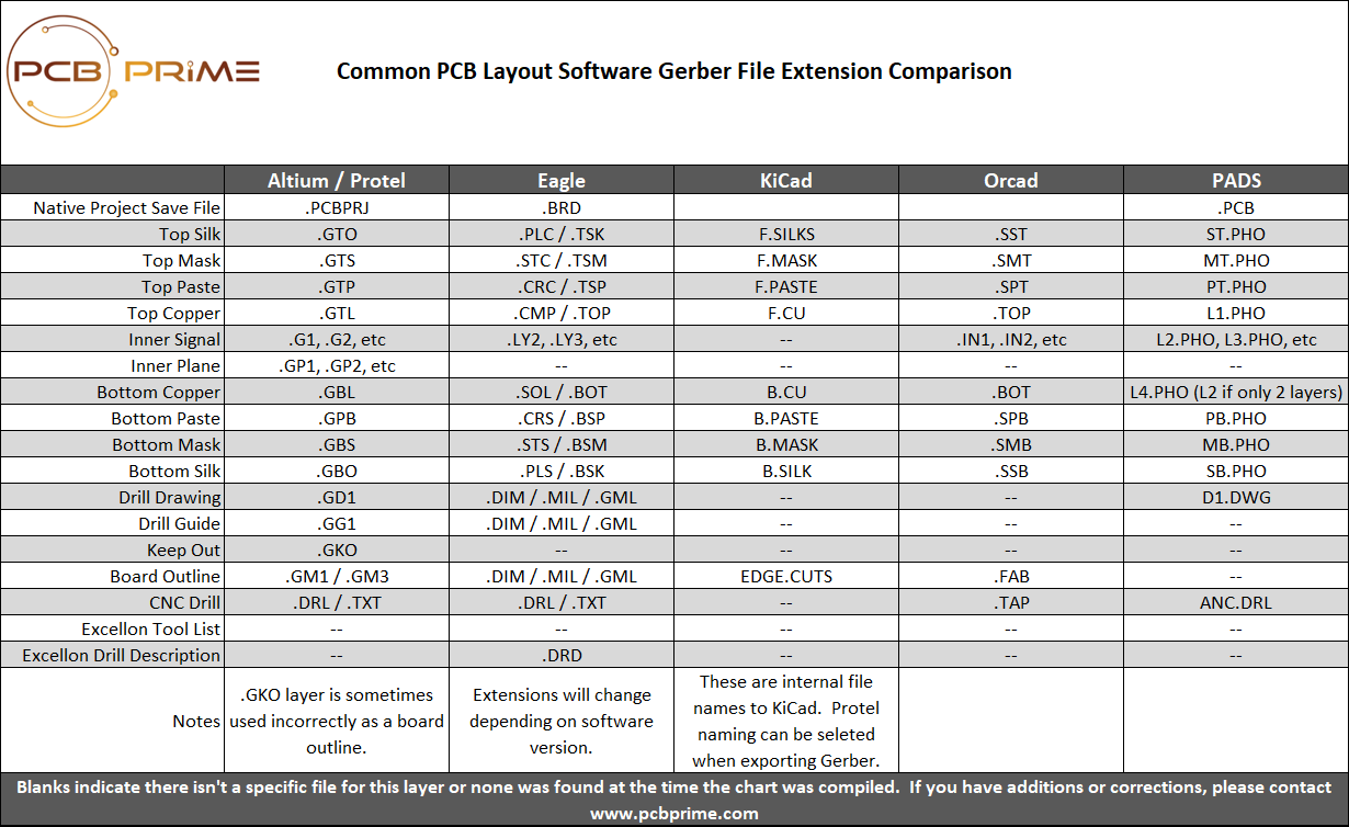
There are dozens of different PCB layout tools on the market which use their own unique naming scheme for Gerber files. Gerber file extensions for some of the most popular PCB layout tools are compared below. Download Gerber File Extension Comparison (PDF)
CNC Drill File
The CNC (Excellon) drill file is the file used to program the CNC drill equipment responsible for drilling the holes in your design. This is a different file format than Gerber. This file is output as simple text and can be read in any text editor such as Notepad, WordPad or Word.
TIP: The most universally accepted format to export your drill file in is: Excellon Format, ASCII Odd/ None, 2.4 Trailing Zero Suppression, English Units, No Step and Repeats.
ODB++
Stands for Open Data Base, the '++', an homage to the C++ programming language, was added in 1997 when component descriptions were added to the output content. With this data standard, there is no need to create a separate CNC Drill file or netlist. The goal of ODB++ is to embed information that is normally found within a fabrication drawing, directly into the file structure. This format is gaining popularity and we have no trouble manufacturing from this format.
The output created with ODB++ is very complex, it creates a myriad of folders and subfolders. Please compress your ODB++ output using a compression tool. For ODB++ files, we recommend 7-Zip, and use either the .tgz or .tar file extension. Standard .zip or .rar compression is also acceptable.
DWG
DWG is a proprietary file format used by CAD systems such as AutoCAD. These tools are not ideal choices for creating PCB layouts and were not designed for this purpose, but some simple designs can be created using these tools. We have successfully converted some DWG files into Gerber RS-274X/CNC Excellon format and manufactured from these files. We need to review them on a case by case basis to see if your file can be converted.
PCB Express (.pcb) This is a proprietary format created from PCB Express's 'Express PCB' software line. As of this writing, we have a tool that can convert this into standard RS-274X/CNC Drill format. We strongly recommend against using "free" fab shop software for layout since the software will only export a proprietary file format only they can open, forcing you to use their service making the software anything but "free".
Files Needed for PCBA (Assembly)
BOM (Bill Of Materials)
This is most commonly called a BOM (Bill Of Materials). A BOM should always be in XLS or XLSX format since this is a common, easy to use flexible format. Each line in the BOM corresponds to a unique component on your board. Click here to download an XLSX example.
The following information is required:
-
PCB Part Number—So we know which board your BOM is for.
Assembly Type—Let us know if you need RoHS assembly or Leaded. We don't want to assume.
Line Number—This makes it easy to reference different lines in the BOM when discussing your design.
Ref Designator—The corresponding Reference Designator as printed in the silk screen on the PCB. Without this, we can't be sure where to place the part. Make sure your board's reference designators are clearly marked.
Qty—The total number of components for this line item used on one (1) PCB.
Internal Part#—Many organizations create internal part numbers for their designs. This is perfectly fine, of course we don't know what your internal part numbers mean so this is listed only for your benefit so there is a cross reference between your part numbers and the official manufacturer part numbers.
Mfg Part Number—Manufacturer's Official Part Number. This is what we search for when ordering your part or researching for data sheets. Make sure your part numbers are complete. The omission of even 1 character can make a big difference in what part shows up in search results.
Description—This is a double check to make sure the manufacturer part number matches what you are intending to use. It also aids in expediting the initial quote process so we can quickly see what types of components need to be installed.
Notes—Any comments you have for this item. Maybe you already have a hard to find part in stock and you're planning on sending it to us when placing the order. Maybe there's a part you want to install yourself or it's not needed on this version. Special care is needed to orient the part correctly or if you already know the best source for purchasing this part.
XYRS / Pick and Place (PNP) / Component Placement List (CPL)
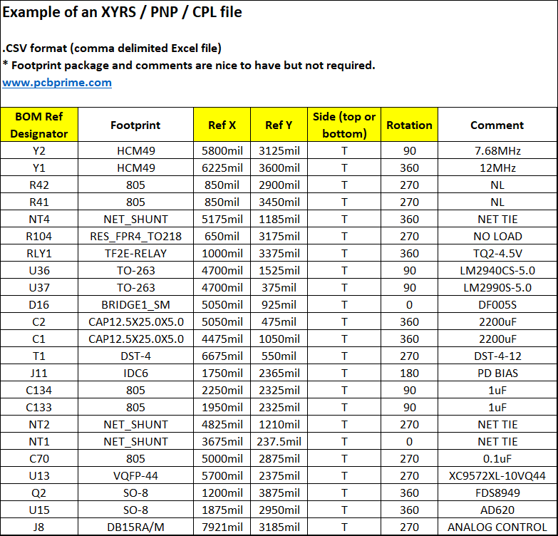 This file is critical when assembling your board. It gives information about the location, rotation and side of the board the part is located. Click here for an example. Your PCB layout software generates this file, this information is not found in Gerber data. This file can be in .TXT, .CSV, .XLS or .XLSX formats.
The file goes by many names, but they all refer to the same file type.
- XYRS (XY coordinates, Rotation of the part, Side of the board the part is on)
- PNP (Pick and Place)
- CPL (Component Placement List)
Critical Information found in this file.
- Reference Designator
- Layer or Side of board the part is located
- X Coordinate for the center of the part
- Y Coordinate for the center of the part
- Orientation, expressed in degrees
Other information that may be included but is not required since this is a file used to program the pick and place equipment and excess information is ignored.
- Part Number
- SMD, Yes or No? Is the part a surface mounted device or a thru hole?
- Footprint type
- Comments showing part values or other notes
Solder Paste Layers
In order to place solder paste in exactly the correct location of your PCB, a stencil is needed. A stencil is a flat stainless steel sheet that has openings laser cut into it to correspond to the surface mount pads on your PCB. The stencil can be anywhere from 2-15mils thick depending on how much solder paste needs to be deposited. The average stencil is between 4-5 mils thick. The thicker the stencil, the more paste will be applied to the board. Stencils are cut using the paste layers from your Gerber data as reference. Paste layers look the same as solder mask layers except they omit any apertures that are not needed for automated pick and placement such as thru hole components.
Even if we are not assembling your board for you, we will step-and-repeat your paste layers as part of our tooling process if they are included in your file set, even though they are not used for the bare board fabrication process.