PCB-TIPS
Accepted File Formats
Array Design
CAM Tooling Guidelines
Controlled Dielectric or Controlled Impedance?
Countersink vs Counterbore
Default Rigid PCB Specs
Dielectric Stacks
Drilling and Drill File
Fabrication Drawing/Fab Print
Fabrication Process
Final Finish Comparison
How Thick Is 1oz Copper?
How to Avoid Engineering CAM Hold
Minimizing Bow and Twist
Solder Mask
Via Tenting, Plugging, and Filling
What is Copper Thieving?
Minimizing Bow and Twist
What Is Bow and Twist?
 Ideally, your PCB should be perfectly flat, however, this is not always possible. IPC has defined the acceptable limits a PCB is permitted to bow or twist, this is defined in IPC-A-600 under section 2.11. Below is an excerpt from IPC-A-600 section 2.11.
(From IPC-A-600 – 2.11 FLATNESS)
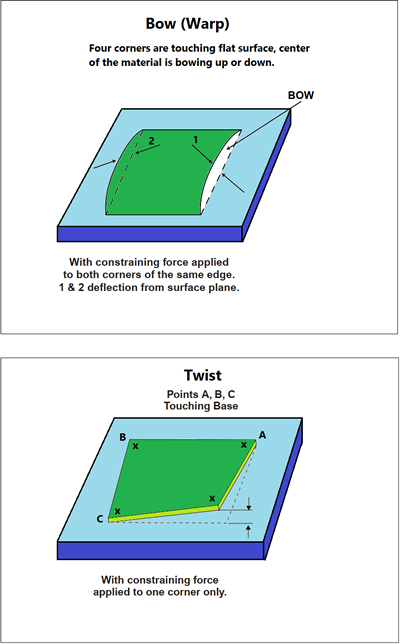
Flatness of printed circuit boards is determined by two characteristics of the product; these are known as bow and twist. The bow condition is characterized by a roughly cylindrical or spherical curvature of the board while its four corners are in the same plane.
Twist is the board deformation parallel to the diagonal of the board such that one corner is not in the same plane to the other three. Circular or elliptical boards must be evaluated at the highest point of vertical displacement. Bow and twist may be influenced by the board design as different circuit configurations or layer construction of multilayer printed boards can result in different stress or stress relief conditions. Board thickness and material properties are other factors that influence the resulting board flatness.
Bow, twist, or any combination thereof, shall be determined by physical measurement and percentage calculation in accordance with IPC-TM-650 – 2.4.22 Bow and Twist. Panels containing multiple boards that are assembled in panel form and later separated shall be assessed in panel form.
Acceptable – Class 1, 2, 3
- For printed boards using surface mount components, the bow and twist shall be 0.75% or less.
- For all other boards, bow and twist shall be 1.5% or less.
To put it in simpler language, a PCB is considered bowed (warped) if all 4 corners can be placed flat on a table and the middle is raised above the table.
Twist is demonstrated by placing the PCB on a table and pressing down on 1 corner. If one of the other corners rises, the material has twist.
IPC-TM-650 – 2.4.22 Bow and Twist
What Causes PCB Bow and Twist?
There are several factors that contribute to the likelihood that a design may bow or twist. Some of the most common are:
- Uneven Copper Distribution
- Unbalanced Stack Up
- Pre-Preg Materials Arranged Incorrectly
- Mixed Material Types
- Finished Thickness
- Moisture
- Rapid Heating During Assembly
- Assembly Conveyor Setup
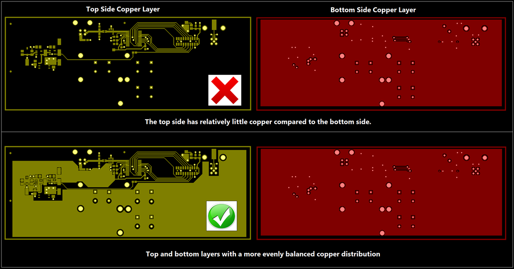
Uneven Copper Distribution
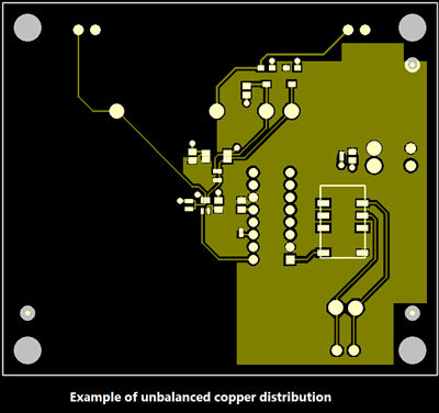 Copper absorbs heat more readily than the PCB laminate. Copper has a comparatively high coefficient of thermal expansion (CTE). If your design has large copper planes or if there are large open spaces with no copper, the copper imbalance may cause the board to flex when heated. Always try to evenly distribute copper across a layer as much as possible. Sometimes copper thieving will be added as necessary to help minimize the likelihood your design will bow or twist.
Also consider the copper distribution on each layer as it relates to the other layers in your design. Issues can arise with your design is one layer has a lot more copper than the others.
Unbalanced Stack Up
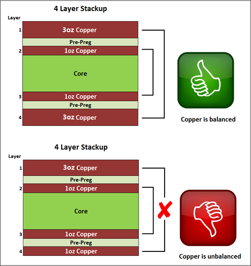 It's a good idea to balance the copper weights (copper thickness) used on each layer in a multilayer design. For example, when designing a 4 layer board, specifying 3oz copper on only one layer and 1oz on the remaining layers would greatly increase the probability of warping.
More information on copper distribution can be found in our How Thick is 1oz Copper article.
Pre-Preg Materials Arranged Incorrectly
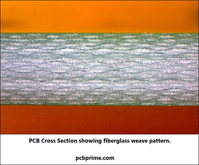 The vast majority of printed circuit board materials in use today are manufactured from an epoxy impregnated woven fiberglass. The weaving process orients the fiberglass strands in 2 directions, perpendicular to each other.
The glass strands laid in the primary direction are under slightly more tension and are called the warp. The strands that are woven in between the warp are called the weft. Before the lamination process, the direction of the warp and weft (grain) should alternate between dielectric layers to reduce the potential the laminate may bow or twist. If every layer is oriented with the warp in the same direction, this tension can compound and result in bow or twist.
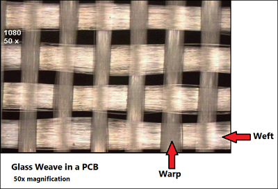 The picture shows how fiberglass strands are woven before being impregnated with epoxy resin.
Mixed Material Types
Designs that incorporate a mixture of different material types in their stack up, such as a Rogers/FR4 hybrid construction, are also prone to bow and twist because each material has a different coefficient of thermal expansion (CTE). Materials with dramatically different CTE characteristics may be flat pre-assembly, but will demonstrate bow or twist after reflow assembly process.
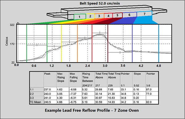
If a mixed material PCB is unavoidable, make sure to use a very gradual heating profile with as many heating zones as possible. At least 7 to 10 zones is recommended for these types of boards with the slowest temperature ramp up you can manage. The more zones and time that can be used for your assembly, the better.
Finished Thickness
Very thin boards are more prone to bow and twist because there simply isn't as much material available to keep the board stiff. The potential for board warp is also increased the longer the board is.
Standard finished thicknesses are 0.062", 0.040", 0.031" (1.6mm, 1mm, 0.8mm). These thicknesses should not be a problem assuming adequate copper distribution guidelines mentioned above are followed. Anything under 0.031" / 0.8mm has a greater chance for warping than thicker boards.
Moisture
The PCB fabrication process requires multiple trips through various chemical baths, rinses and washes. It's easy for liquid or gasses to become trapped within the fiberglass weave or inside plugged or tented vias. One of the final steps in the PCB fabrication process is to bake the boards at a low temperature (248°F – 266°F / 120°C – 130°C) for several hours while inside a press. It is still possible for moisture or gasses to remain trapped inside the board even after this process, but it should be minimal at this stage.
It's also possible for moisture to wick into the board simply by absorbing the ambient humidity in the air. If you are storing boards on a shelf for any amount of time, it's advised to reseal any open board packs with a desiccant, not only to prevent unwanted moisture but also to slow the degradation of the surface finish.
TIP: At PCB Prime, we will package your boards in an airtight shrink wrap along with a desiccant to prevent moisture absorption during transit or storage.
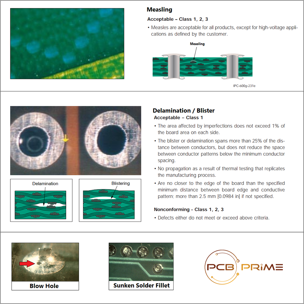
During assembly, any trapped liquids or gasses will try to escape when the board is heated to reflow temperatures. This evacuation is called outgassing. In extreme cases, outgassing can cause components to be physically ejected from the board during the assembly process. Outgassing may also cause other damage such as measling, delamination, blow holes, and sunken solder fillets.
(From IPC-A-600G)
Measling manifests itself in the form of discrete white squares or "crosses: below the surface of the base material, and is usually related to thermally induced stress. Measles are subsurface phenomena that have been found in new laminated materials and in every board type made from woven fiber reinforced laminates at one time or another. Since measles are strictly subsurface phenomena and occur as a separation of fiber bundles at fiber intersections, their apparent positions relative to surface conductors have no significance.
Delamination is a separation between plies within a base material, between a material and conductive foil, or any other planar separations within a printed board.
Blister is a delamination in the form of a localized swelling and separation between any of the layers of a lamination base material, or between the base material and conductive foil or protective coating.
Blow holes are demonstrated by small voids in through hole solder joints. If the copper plating in the barrel of the holes is thin, weakened, or cracked, it can allow gasses to escape during assembly.
Sunken Solder Fillets can be caused by outgassing caused by trapped moisture or gasses escaping the laminate during assembly. If the copper plating lining the hole wall is at or above the IPC standard 25µm, then the copper should prevent outgassing. Other causes for sunken solder fillets are:
Incorrect hole to lead size ratio, where the component lead is not large enough to support the weight of the solder. There won't be enough solder to fill the hole above the surface of the laminate.
Contamination or foreign inclusion in the hole preventing proper solder flow.
Improper heating or insufficient flux.
Rapid Heating During Assembly
 The slower your board is heated during solder reflow the better. This will allow the copper and laminate to expand at closer to the same rate and prevent the board from bowing or twisting. Copper has a higher CTE (coefficient of thermal expansion) than laminate.
A successful lead-free solder process requires higher temperatures and has tighter target ranges for heating, cooling and time spent in each zone. It's recommended to use a reflow oven with as many zones as possible to dial in your reflow profile. An oven with at least 7 zones is recommended for lead free assembly process.
Assembly Conveyor Setup
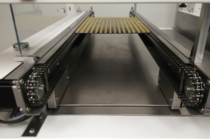 Modern assembly equipment will generally use a conveyor system to transport boards through the assembly process. If the conveyor is a side rail system, it's possible the spacing is too tight and it's placing stress on the board causing it to bow. Check to make sure your conveyor system is uniformly parallel along the entire length of the track. The spacing may be perfect at one end but may start to widen or become tighter in other places.
If your system includes a center support, also check to make sure the support's height is consistent across the entire track.
How Do I Measure To Check If My Board Exceeds IPC Bow and Twist Criteria?
The testing criteria are outlined in the IPC-TM-650 document, section 2.4.22 which can be viewed for your convenience below.
-
Boards that contain surface mount components, should have bow and twist at 0.75% or less.
-
All other board types should be 1.5% or less.