PCB-TIPS
Accepted File Formats
Array Design
CAM Tooling Guidelines
Controlled Dielectric or Controlled Impedance?
Countersink vs Counterbore
Default Rigid PCB Specs
Dielectric Stacks
Drilling and Drill File
Fabrication Drawing/Fab Print
Fabrication Process
Final Finish Comparison
How Thick Is 1oz Copper?
How to Avoid Engineering CAM Hold
Minimizing Bow and Twist
Solder Mask
Via Tenting, Plugging, and Filling
What is Copper Thieving?
PCB Fabrication Drawing/Fab Print
At PCB Prime, we don't require a fancy fabrication drawing. A simple readme.txt works just as well. We can accept just about any standard format for your fabrication notes. Popular fab print file types we can use are:
| .TXT | .PNG | .JPG | .DXF | .XLS | |
| .DWG | .DOC | .PPT | .XLSX | .DOCX |
TIP: If placing an order online, please let us know if you are intentionally ordering a different specification than is referenced in your files. Your order will go on engineering hold if we find a conflict between the specifications you order online and what we find in the fab print.
A lot of information can be conveyed in a fab print, below are the most common elements of a standard bare board PCB fabrication drawing.
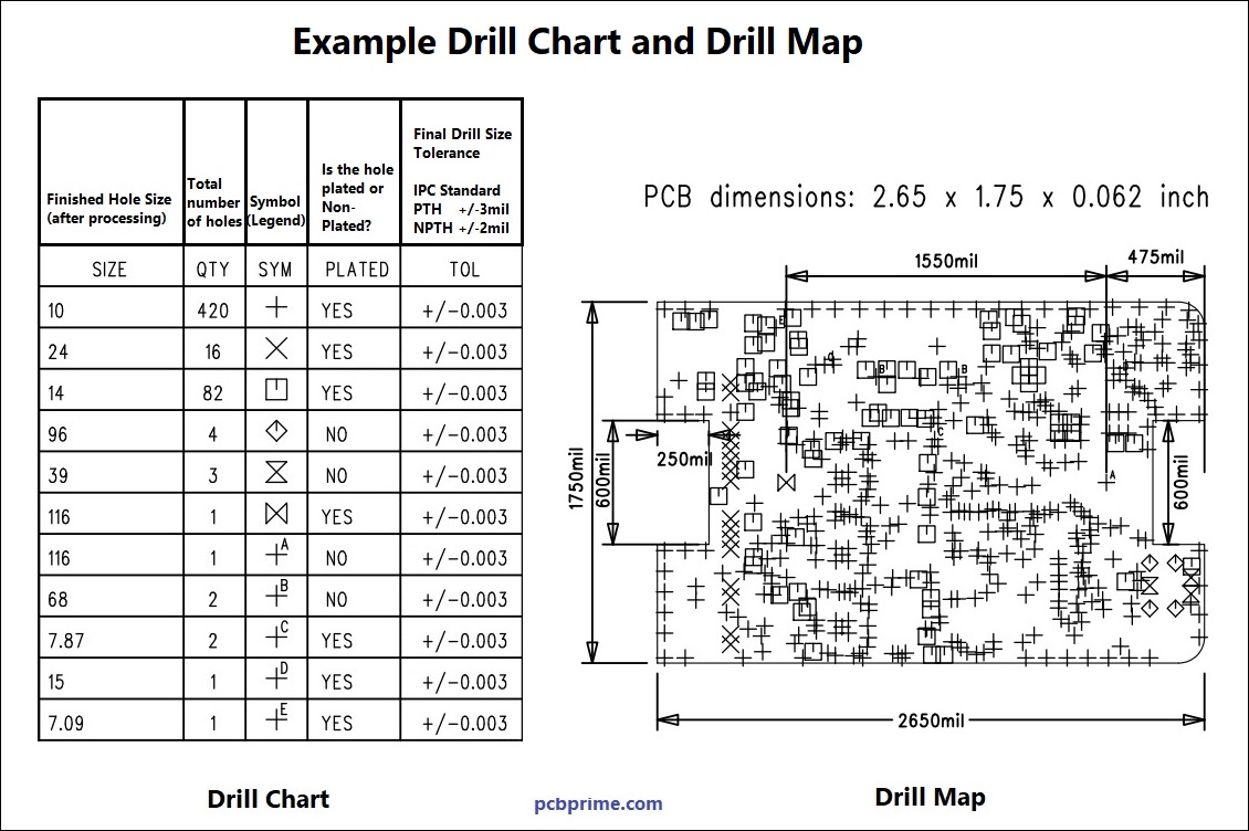
Drill Chart
This is a simple chart showing the relevant information about the holes and slots that are to be drilled or routed in the PCB. Typical information shown.
- (Finished) Size - The size the hole or slot should be after copper plating and final finish are applied.
- Quantity - The total number of drill hits made at this size.
- Symbol - Each tool (drill) size is assigned a unique symbol to make it easier to determine the intended location and size of your holes. These symbols are used on the drill map described in the next section.
- Plated - The attribute of the hole. Either PLATED (PTH) or NON-PLATED (NPTH).
- Tolerance - The accepted tolerance range for the finished hole size. IPC Class 2 standard is ±3 mil (0.076mm) for PTH and ±2 mil (0.05mm) for NPTH. Upon request we can accommodate a ±2 mil PTH tolerance for press fit connectors for a small additional charge.
Drill Map
This a good companion to the drill chart. This allows the CAM operator to perform a reality check against your CNC drill file and make sure all holes are in the correct location and the correct tool size.
Board Origin
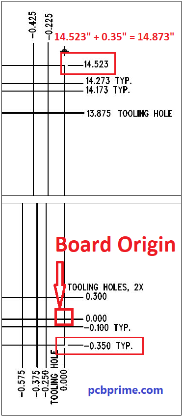 The board origin is the location where all dimensional and positional measurements are relative to. Usually the lower left corner of the PCB is set as the origin or 0,0. Ironically, the example I chose for this example has the origin set at the lower right corner.
This example is calling for the addition of tab routed tooling rails, the origin is set at the lower right corner of the board itself, not the lowest right corner of the tooling rail. The designer could have set the origin at the lowest right corner of the tooling rail but they chose to set the origin at the lower right corner of the PCB. Be careful when reading fabrication drawings and make sure you are accounting for any negative numbers that may be used when the origin is not set at the farthest corner of the drawing.
In this example, the lower rail is -0.35" below the edge of the board. The correct length of this board in the Y axis is 14.873", not 14.523". You would need to add 0.35" to the dimension shown at the top right edge to know the correct total length.
When working with your data for tooling purposes, we will automatically reset your origin to the lowest left most corner of the design, including any additional tooling rails. This not something that will affect the design in any way, it is for our internal processing only.
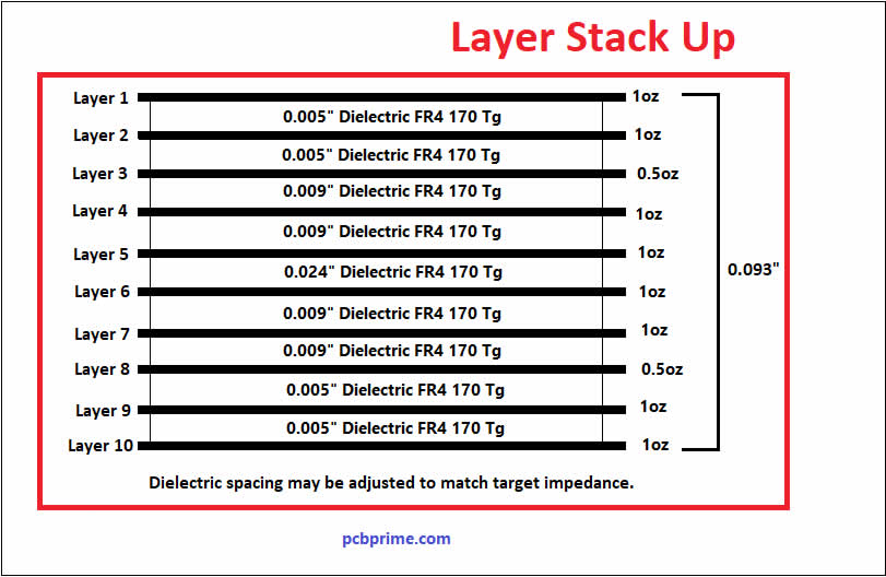
Layer Stack Up
A layer stack up serves many functions. If your design is only one or two copper layers, a stack up is generally not necessary. For designs with more than two copper layers, a stack up is a concise way to relay a lot of information. This information may include things such as:
- Layer Stack Order – What order the internal layers should be placed.
- Dielectric Spacing – The amount of material needed to separate the layers.
- Copper Weight – Amount of copper required per layer.
- Type of Material.
- Overall thickness of the finished board.
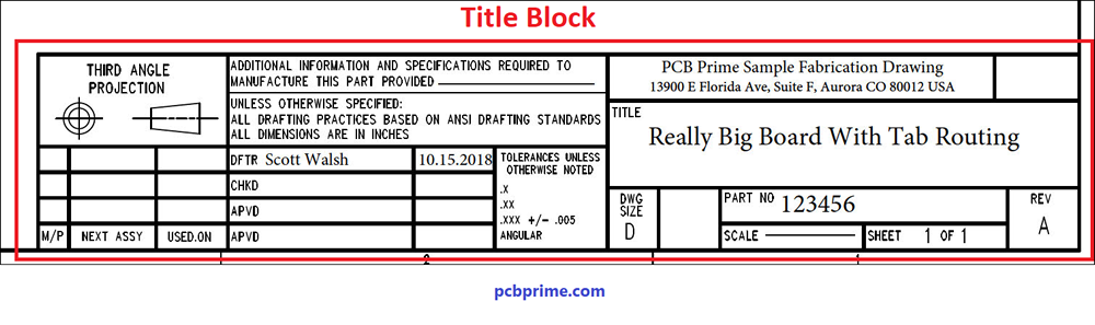
Title Block
A title block is not required but it can be handy to have. Generally, the correct part number and rev is given as well as contact information for the PCB designer and the units of measure.
TIP: The importance of indicating the correct part number and rev cannot be overstated. Frequently we have no choice but to guess as to what to call a board simply from what we see printed on the silk screen or based on the name of the zip file. It can be very confusing to try and locate a past quote or order when a board can go by several different names or descriptions.
Special Note Call Outs
If there are areas of interest that need closer attention, it's a good idea to indicate this on the fabrication drawing.
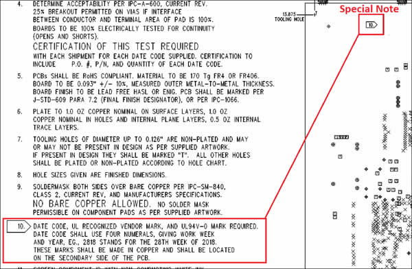 In the example here, the note calls for UL/Date Code information to be placed in a specific location on the PCB. The note number has an arrowed box around it and the same box and note number is found on the drawing indicating where it should be placed.
This technique can be used to draw attention to anything that may be non-standard and could otherwise be missed. As you can see, sometimes fabrication drawings can contain a lot of information so it always helps if 'unusual' instructions are highlighted in some way.
Sometimes There is Too Much of a Good Thing in a Fab Print
When you've read as many fabrication drawings as we have, sometimes the most important details can be missed when it's buried among a lot of other information that's either industry standard, common practice, a restatement of IPC standards, or irrelevant to the bare board manufacturing process.
We've seen fabrication drawings that are 6 pages long, specifying IPC criteria for every imaginable aspect of the board. Typically, 98% of this information will be standard industry practice and is a restatement of IPC standards and doesn't need to be specifically stated. However; we still need read through all the information in case there is something unusual buried in the notes. If you want your board manufactured to the latest revision of IPC-6012 with a Class 2 inspection, that's all you need to state. (95% of the boards we build fall within this category). Citing IPC criteria for every aspect of the bare board construction is redundant and may cause more important details in your fab print to be missed.
At PCB Prime, our default manufacturing and inspection process is as follows.
| IPC-6012 current rev | Qualification and Performance |
| IPC-A-600 current rev | Acceptability of Printed Circuit Boards |
| IPC Class II | Inspection Criteria |
Ideally, your fab print should only identify specifications that run counter to the IPC Inspection Class or other standards mentioned in the fab print. The most common bare PCB specs are listed in the Rigid PCB Default Specifications. If you require any special processing such as Controlled Impedance, Blind/Buried Vias, Via In Pad, Counter Sinks/Bores, Plugged Vias, Cutouts in the board, etc; please state these requirements in a fab document since we can't necessarily tell these requirements exist from reviewing the raw board layout.