PCB-TIPS
Accepted File Formats
Array Design
CAM Tooling Guidelines
Controlled Dielectric or Controlled Impedance?
Countersink vs Counterbore
Default Rigid PCB Specs
Dielectric Stacks
Drilling and Drill File
Fabrication Drawing/Fab Print
Fabrication Process
Final Finish Comparison
How Thick Is 1oz Copper?
How to Avoid Engineering CAM Hold
Minimizing Bow and Twist
Solder Mask
Via Tenting, Plugging, and Filling
What is Copper Thieving?
PCB CAM Tooling Guidelines
When we receive artwork for a printed circuit board, many things are checked and adjusted to ensure the board is fabricated as closely as possible to the original design. If we notice something that appears unusual, we'll hold the order and question the designer's intent.
Since a PCB can be drawn up in ways that are not possible to physically manufacture, we perform a free DFM (Design For Manufacturing) review on every order before releasing it to the production floor. We have seen every design rule set imaginable. Over the years we've made boards for everyone from hobbyists to fortune 500 companies, so we've seen the full spectrum of experience, design techniques, and software packages.
There are many steps to tooling a board for production. The average design takes around 1.5 - 2 hours of engineering time to review, align and adjust all the things needed to ensure your board is manufactured as closely as possible to the intended specification.
CAM Review Overall Check List – Bare Board Fabrication
Below is a brief summary of what our CAM (Computer-Aided Manufacturing) engineers will review when "tooling" your board for manufacturing. We will review the board for any design rule violations that are not manufacturable and anything that looks out of the ordinary.
Fabrication Print Review
- Ensure the fabrication drawing specifications match the sales order and Gerber.
- Are all specifications in the fab drawing achievable?
- Do the dimensions in the drawing correspond to the actual measurements in the digital file?
- Are there any instructions that are unclear or not manufacturable?
Alignment and File Verification
- Verify all required digital files are present and accounted for.
- Align and orient all layers.
Copper Layers
- Verify copper to copper spacing meets the min requirement based on the desired copper weight.
- Copper is not overlapping the board edge (unless this is intentional).
- No dead-end trace fragments.
- Board outlines or other extraneous information outside the board perimeter are deleted.
- Copper features are scaled up to account for etch and plating processes.
- Compare drill file to outer copper layers to ensure any plated holes have adequate copper surrounding the hole.
- If gold fingers are present, traces are added to the ends of the fingers to tie them to the buss bar for the electrolytic hard gold plating process.
- On inner layers, non-functional copper pads around vias that do not connect to the layer are removed.
Solder Mask
- Adjust solder mask swell to meet a 4mil - 5mil oversize mask clearance. (2mil to 2.5mil per side of the copper feature.)
- Verify there is enough spacing between copper features to reliably print mask dams.
- Inspect the board for any potentially missing solder mask clearances and question clearances that don't seem correct.
- Board outlines or other extraneous information outside the board perimeter are deleted.
Silkscreen
- Verify silk screen line width and character height meets minimum requirement for legible printing. We'll adjust or send you an FYI as necessary.
- Re-locate or clip silk screen that is too close to a solderable surface.
- Board outlines or other extraneous information outside the board perimeter are deleted.
Drill File
- Verify drills are centered within their copper pads.
- No apparent missing drill hits.
- Duplicate drill hits are deleted.
- Customer specified drill hole tolerance is achievable (IPC Class 2 Standard +/- 3mil for PTH and +/-2mil for NPTH).
- Edge of drill to edge of drill spacing meets the minimum requirements.
- If supplied, compare drill chart and drill map to the actual CNC drill file.
Board Outline
- Verify outline is congruent with fab drawing and sales order. We follow industry standard practice for determining the true edge of the outline. We use the CENTER of the line used to draw the outline as the true edge.
- If there are outlines on multiple layers of data supplied, we will use the .GM1 layer or another mechanical layer as the correct outline. Please note, .GKO is technically a keep out layer but this is often mis-used as an outline layer. We will use the .GKO layer only if no other outline is provided.
- If there are any cut outs or slots that need to be routed in the board, these will be added to the mechanical board outline layer.
- CNC route file is created.
UL/Date Code/94V-0/RoHS Markings
- If requested, we will add UL/Date Code/94V-0/RoHS markings to your board.
- If no request is made, our default is to not add any additional markings to the board.
Additional Checks on Multilayer boards (boards over 2 layers)
- Verify a layer sequence is provided.
- If the fab print specifies a stack-up (controlled dielectric), verify it can be met with materials on-hand.
- Controlled Impedance, verify the calculations and suggest changes to the design as needed to meet target impedance.
Creating Arrays (Panels)
- Follow customer requirements for panelizing the design or designs into an array for easier automated assembly.
- Add tooling rails, fiducials, tooling holes, scoring, and tab routing as needed for the array.
- Paste (stencil) layers are not required for our bare board manufacturing process, we will panelize the paste files along with the other files in the array as a courtesy, so you can get a stencil manufactured. Have your stencil shop review these layers carefully since we are not adjusting these files in any way, we only step and repeat them as they were submitted to us. Don't forget, we also manufacture stencils!
File Creation (Tooled / Working File)
- After everything has been reviewed and adjusted, the finalized "working file" is created and uploaded to our server. An email with a link to download this file will be emailed to you.
- All our boards are electrically tested based on an optimized net list generated from your original file. If an IPC netlist is also supplied, we will compare the IPC file to the Gerber to ensure there are no discrepancies.
- The appropriate files will be distributed to the various manufacturing departments so they are ready when your order passes through each department.
Below is a more detailed explanation of some of the main points covered in the CAM review process.
Read the Fab Print
You'd be surprised how many circuit board designs we receive that contain very little to no information regarding the specifications of the circuit board. How thick the board should be, copper weight, the final finish desired, even the color of the mask and silk screen. If there are no instructions in the files, we assume the following industry standard specifications when quoting and building your order.
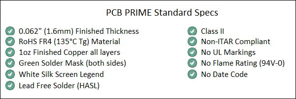
TIP: Even if these standard specifications match how you'd like your PCB constructed, it's always a good idea to state this either in a fab layer in the Gerber or in a readme.TXT, PDF, DOC(X), XLS(X), or DWG file. This way there's no question as to how your board should be constructed.
PCB Prime Fabrication Drawing Example.pdf
Comparing Fabrication Drawing to Gerbers and Drill File
If a fabrication drawing is provided, we will compare this drawing to what we see in the digital layout. We double check dimensions, hole placement, hole sizes, quantity of holes, spacing between features, and any other items we can compare.
Verify All Required Files Are Present
We will verify at least the minimum number of files necessary to manufacture a PCB are present. If a fab print or other design information is not supplied, we will assume the files that are submitted are all that is required. For a standard 2 layer circuit board, we will need at least these files.
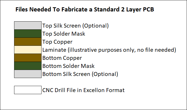
- Silk Screen files are optional so we will not question it if your design doesn't include these files.
- Solder Mask files tell us where to print the solder mask. Most PCBs will require solder mask on both sides of the board so we'll need a separate mask file for the top side and the bottom side. If your design doesn't require solder mask or if you want mask to completely cover the entire board, please let us know so your order does not go on hold for a missing file.
- Copper layers are required for each layer of your board that contains copper. We have made many boards that are used as face plates or for other mechanical purposes, so it's possible you may not need copper on your design. If copper isn't needed, or if you have copper on only 1 side, please let us know.
- CNC Drill Files are by far the most commonly forgotten file. Depending on your software package, this file is sometimes generated in a separate step from the Gerber files, so it's easy to forget to include it. This file is used to program the CNC drilling machines so even if you have a drill map in Gerber format, this is not the correct file format for CNC drilling. We need a drill file in CNC Excellon format. If your design has no holes, please let us know so we know don't assume this file is missing.
Aligning the Layers
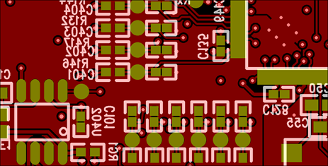
Sometimes we receive files where the layers aren't aligned relative to each other, so our CAM engineer will check and realign all layers. During this step, the engineer will also verify the layers are oriented the correct way. Industry standard is to view files as if looking at the board from the top side through to the bottom of the board. This means any text on the bottom layers should appear backwards (mirrored). It's necessary to view files this way so we can ensure all drills are aligning correctly. The image below is a screen shot showing how the bottom side of the board will look when viewed from the top side.
Copper Compensation
Very simply, every copper layer of a PCB begins as a solid sheet of copper. The image we see in your design files is photo plotted onto a film and then transferred to an etchant resist that protects the copper only in areas where the copper is to remain. To reveal your design, the excess copper is etched away by submerging the entire panel into a chemical solution.
As soon as the chemicals begin etching down toward the laminate, they also begin etching laterally underneath the resist. Since the copper closest to the resist will be exposed longest, these areas will have the most lateral etching resulting in a trapezoidal shape. As you can imagine, the thicker the copper, the more time it will take for the solution to etch all the way down to the bare laminate to define your pattern.
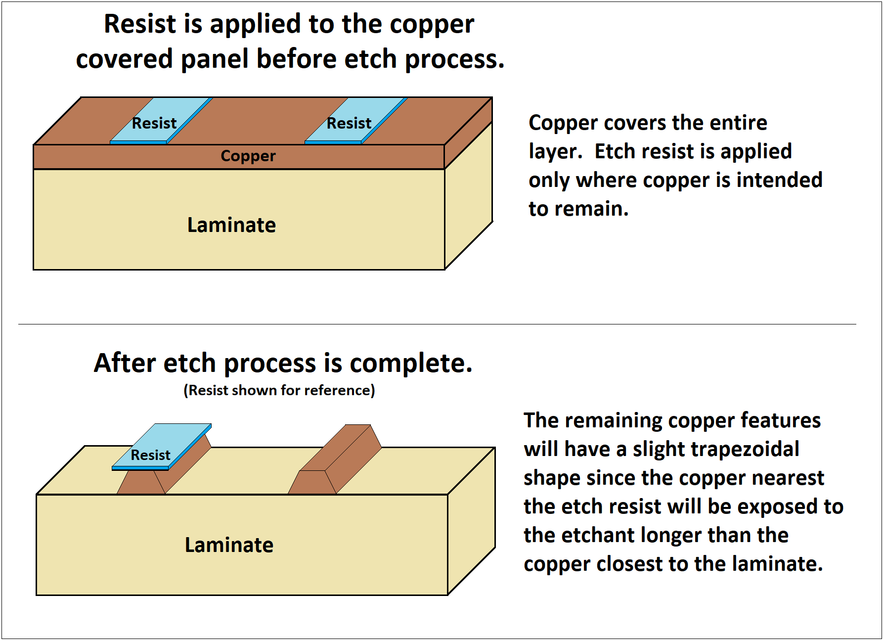
To combat this phenomenon, copper features will be enlarged slightly to compensate for the etch process. If we printed the copper pattern at an exact 1:1 ratio between what we see in the computer vs the actual printed image, your copper features would end up being slightly smaller than desired. The amount of compensation needed is dependent on the amount of copper being etched (how thick the base copper is on the laminate) and the copper distribution on your design. The thicker the copper, the longer the laminate will be submerged in the in the etchant tank. The goal is to calibrate the enlargement so the features will be as close as possible to the sizes in the original artwork. This compensation will initially reduce the spacing between copper features during imaging and production. This is one of the primary reasons why higher copper weight designs require more space between the copper features. We need to be able to enlarge the copper features more than usual to compensate for the extra time the board will be in the etchant solution.
Again, this is not something you need to worry about but, as a general rule, these are the amounts copper features are enlarged to compensate for etch.
1oz copper = 1.5mil (0.038mm) copper feature overall enlargement
2oz copper = 3mil (0.076mm) copper feature overall enlargement
Solder Mask Clearances
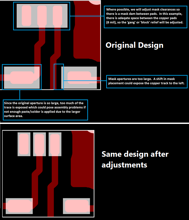 We will automatically adjust the mask clearances so they are 2-2.5mils larger on all sides of the copper pad. If there are spacing concerns, then we may adjust the mask swell to as little as 1-1.5mil per side.
Solder mask has a true positional tolerance of +/- 2mils (+/-0.05mm). We see many designs where the mask relief aperture is the exact same size as the copper pad it's exposing, or sometimes much larger than the pad. If we build a board with mask apertures the same size as the pad, there would be a very good chance the mask would not be in perfect alignment with the copper and some mask would be printed on the pad reducing solderability.
If we leave the mask aperture much larger than the pad, there's a chance adjacent copper may be exposed which could result in solder bridging to another net after assembly.
Sometimes we see what is called a "solder mask defined pad". This is when the mask clearance is intentionally smaller than the copper pad and is typically used when spacing is very tight, making it impossible to print mask between the pads using a traditional oversized mask aperture. Please let us know if our design contains any solder mask defined pads so we know how to process these areas.
TIP: By default, we assume all solder mask apertures should be larger than the copper pad.
Silkscreen Clipping
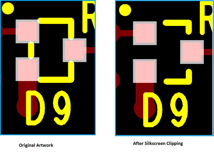 Since silkscreen on a solder pad would make it difficult to solder, we will move silkscreen when possible or clip (delete) the portion of the silkscreen that is too close to the pad.
TIP: Min distance required for silk screen to exposed copper pad is 5mils.
Drill Size Compensation
When a drill size is specified in original artwork, it's industry standard to assume the sizes listed are finished hole sizes. In other words, it's the size the holes should be after fabrication is complete. Since plated thru holes (PTH) will have plating lining the inside of the hole walls, the holes need to be drilled slightly larger than the intended finished size to account for the plating and final finish. (A standard board will have an average minimum hole wall copper plating thickness of 0.79mils (0.02mm/20µm/789µin.) The hole wall compensation also depends on the final finish selected since different finishes plate at different thicknesses and they will also line the hole walls, affecting the finished diameter of the hole.
The degree of compensation is not something you would need to worry about since our CAM engineers will scale the holes for you to reach your intended target size. For those of you who are curious, assuming standard processing and 1oz copper, here are the typical compensations made to the hole sizes.
| Solder (HASL) finishes will have | +6mil/(0.15mm) drill size compensation |
| All other surface finishes will have | +4mil/(0.10mm) drill size compensation |