PCB-TIPS
Accepted File Formats
Array Design
CAM Tooling Guidelines
Controlled Dielectric or Controlled Impedance?
Countersink vs Counterbore
Default Rigid PCB Specs
Dielectric Stacks
Drilling and Drill File
Fabrication Drawing/Fab Print
Fabrication Process
Final Finish Comparison
How Thick Is 1oz Copper?
How to Avoid Engineering CAM Hold
Minimizing Bow and Twist
Solder Mask
Via Tenting, Plugging, and Filling
What is Copper Thieving?
Solder Mask
What Is Solder Mask?
Most boards today are manufactured using LPI (Liquid Photo Imageable) solder mask. Unless otherwise instructed, we will always use an LPI solder mask for your order. This is the easiest, most cost effective, and for most designs, the best type of mask to use.
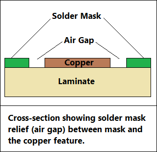
LPI mask is an epoxy-based polymer that is applied over the entire PCB surface, top and bottom, and cured with a high intensity UV lamp. The UV light passes through a clear film containing darkened apertures over the areas where you don't want the mask to adhere to the board. Since these darkened areas won't allow light to cure the mask behind them, the uncured mask can be washed off leaving mask only where necessary. Registration tolerance on the LPI mask process is ± 2mils (± 0.05mm).
Why Do I Need Solder Mask?
 The use of solder mask has several advantages. The most noticeable benefit of is that it makes your board look good! Ok, that's not its most critical job, but depending on your application, it might be.
For most designs, the most important role solder mask plays is to protect the board from corrosion due to environmental exposure and prevent accidental short circuits during assembly or use. Anyone who's ever wielded a soldering iron knows that solder tends to flow away from where you want it to go, so mask not only helps protect the board from accidental short circuits, but it also creates a slightly raised boundary that helps to keep solder contained in the desired location. We recommend that you cover the entire board with mask except those areas where you need to solder or if you need access to a test point.
How LPI Solder Mask Is Applied
- The outer layer copper features have already been etched, drills are drilled and plated through.
- The panel is cleaned to ensure an ideal surface to bond to. Most solder mask processing is done in a clean room environment to prevent debris from getting on or under the mask.
- The panel is completely covered on both sides with uncured liquid mask. The panels are placed in a rack stand so they remain vertical through the process.
- The panel is placed in an oven to tack dry so it won't run.
- The panel is exposed to a high intensity UV lamp to cure the mask. The light passes through a film that is precisely aligned with the panel. The film is clear in all areas where mask should cure and adhere to the board. In areas where mask is not wanted, there are darkened apertures printed on the film that have been extracted from the mask layers in the customer supplied design files. The dark apertures will block the UV light from curing the mask underneath.
- The panel is checked for proper mask alignment.
- Uncured mask is washed away in the developer.
- The panel is taken out of the clean room and placed into an oven to completely cure and harden the mask. Silk screening the legend is the next step in the manufacturing process.
How Do I Remove Solder Mask From My Board?
It happens, sometimes a mistake is made with the original artwork and something gets covered with mask that shouldn't be. Before sending your files in for manufacturing, turn on your top copper and top solder mask layers at the same time to make sure everything that needs to be open in the mask layer is open. Do the same for the bottom layer. Sometimes we can catch things that are look questionable, but sometimes the designer's intent isn't clear. Solder mask is very difficult to remove once cured.
- TIP: It's also a good idea to check your paste layers against the copper and mask layers to make sure everything that's open in the paste is also open in the mask layer and vice versa. You don't want to get your boards and assembly stencil manufactured to find out you forgot to leave and area on the board uncovered with mask, or are missing an opening in your stencil.
Chemical Stripping
There are some chemical strippers that can be used to remove mask, but generally speaking, anything strong enough to remove mask will also damage the copper and laminate underneath so be very careful not to expose the board for too long. Most chemical strippers that will work will contain methylene chloride.
You'll want to tape off the surrounding area on the PCB to keep the chemical agent localized to your target area. If you have a lot of boards to do or a lot of fine pitch areas, you may be better off reordering the boards with the corrected mask file. The amount of time and effort required to strip the mask may be more expensive and messy than remaking the board.
Physical Scraping
A Dremel is a wonderful tool. If you have a steady hand and the right bit for the job, a Dremel (or something like it), will take mask off quickly. Of course, it's very easy to remove more than intended. Copper on most designs is only 1oz (1.37mil) thick. Sometimes a razor or X-Acto knife may be a better option. It all depends on your specific situation.
What Is Dry Film Solder Mask?
Before LPI masks were invented, solder mask used to be applied as a sheet of film that was adhered to the surface of the board with pressure and heat. It's rarely called for these days. If we do see it specified in a fab print, it's almost always on a very old legacy part that hasn't had its fabrication print updated in years.
Dry Film Advantages
- It can be very accurately placed and aligned so very dense designs may benefit from a dry film.
- Since it's a film, the mask will not wick down into the holes like an LPI application can.
- A film provides a more 'air tight' design. Some bare board testing processes utilize a vacuum to keep the board in place. If dry film is used to cover vias, there is better suction on the board.
- Since dry film is prefabricated on a roll, there is less opportunity for the film to become contaminated posing solderability issues.
Dry Film Disadvantages
- It's more expensive than the far more common LPI mask process.
- Dry film is thicker than LPI. It's usually between 3mil - 4mil (0.08mm – 0.1mm), where LPI is usually between 0.8mil – 1mil (0.02mm – 0.025mm). This extra thickness may cause issues aligning fine or shallow parts.
- Dry film follows the contours of the traces and copper features so it will be slightly raised over copper. Liquid Photo Imagable masks are applied as a liquid so the surface is naturally smoothed and leveled.
- Dry film doesn't handle high temperatures well. It can easily crack or peel when exposed to higher temperatures or repeated thermal cycles.
- Vias covered by dry film can trap gases inside the hole which can outgas, rupturing the film during assembly or functional temperatures.
- Proper application of dry film is tricky. The curing temperatures and duration need to follow a tight tolerance or the film can be easily compromised.
Solder Mask Color Options
By far the most common solder mask color is green but many other colors are available. The most common colors we use at PCB Prime are listed below.
| Green | Matte Green |
| Black | Matte Black |
| Blue | Matte Blue |
| Red | Yellow |
| White |
Solder Mask Color Consistency
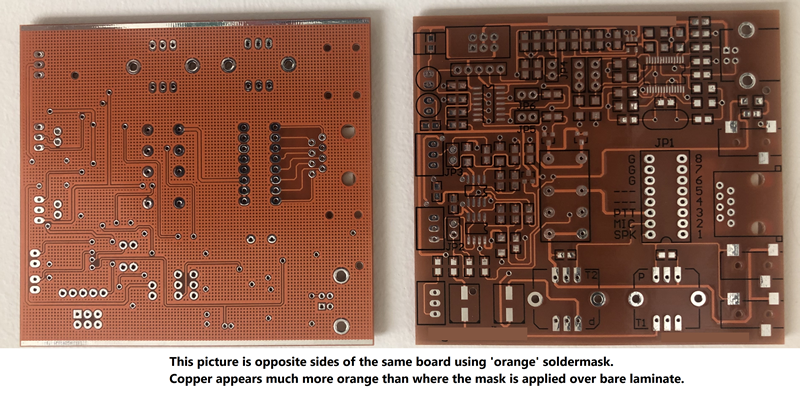
We've tried to match colors in the past and found it's nearly impossible to do. The exact same mask can be applied to different designs and the color will look quite different depending on the copper distribution on the board. Generally, areas where mask is covering bare laminate will appear darker and deeper than areas where it's covering copper.
Custom Colors
We can mix custom colors by mixing standard colors to make such shades as orange, pink, purple, etcetera. Please be aware that custom colors are usually created by mixing 'standard' mask colors by hand, so getting the exact same color balance for orders made several weeks or months apart is impossible. Unfortunately, there aren't automated solder mask mixing machines like you may have used for paint at places like Home Depot or Sherwin Williams. We will do our best to keep the color as consistent as possible but expect some variation from order to order when using a custom color.
Another reason for color variation is that PCB factories will sometimes purchase mask materials from different suppliers due to cost or availability, the exact shade will differ from supplier to supplier.
Why Are PCBs Usually Green?
There are many theories as to why green became the default PCB color. No one seems to know for sure which is correct, maybe it's due to a combination of factors or something that no one knows or remembers. The top theories are listed below.
- Green was the best-looking color possible given the process at the time. The original chemistry for solder mask comprised of a base resin that was a brown/yellow and a darker brown hardening agent was added to cure the mask. Attempts were made to add different combinations of pigments to the mixture, but reds and blues just got darker, were not very attractive, and made it difficult to see the circuitry underneath. The best result was achieved by adding yellow and a touch of blue to make green.
- Green mask is the best performing color. Because green became the default color early on, mask manufacturers placed more focus on finetuning green for optimal performance. One of the most important characteristics for a solder mask is adhesion to the PCB laminate. Good adhesion allows the ability to print very narrow mask dams between tight SMD pads. Green also reacts very well to UV exposure, which is the process that cures and bonds the mask to the laminate.
The best performing colors in order are:
Color Min Mask Dam Width Green 4mil (0.10mm) Blue 5mil (0.12mm) Red 5mil (0.12mm) Black 6mil (0.15mm) White 6mil (0.15mm) - Green reduces eye strain, especially when inspecting boards. As anyone that has ever worked in Quality Control can attest, it's exhausting looking closely at anything for hours on end searching for imperfections. Green has been shown to psychologically have a calming effect and it provides good contrast between traces, pads, and areas of no copper. This makes defects easier to spot and reduces fatigue.
- Cost. Anytime there's a standard or 'most popular' of anything, economies of scale invariably start kicking in. Since most boards are made with standard green, the production line is optimized for this color. Other colors are possible but in order to use a different color, the equipment must be cleaned, calibrated, and prepped for the color change. LPI mask is a messy liquid process and different colors can't be swapped on the fly. This takes time which results in a higher cost. Of course, you could have a separate mask line for different colors, but this is likely cost and space prohibitive in some factories.
Today, most PCB factories batch similar spec PCBs onto the same production panel to optimize material yield and streamline production. If there were 6 different popular colors, the ability to combine different orders together in this way would be much more difficult since different color boards can't go through the same mask process.
How Do I Know If My Solder Mask File Is Correct?
The best way to review where mask will be applied is to look at your top copper layer and your top mask layer at the same time. They should be aligned so you can see exactly where mask clearances will be in relation to the copper. Anywhere you see a mask pad on the mask layer is where mask will NOT be applied. Do the same review for your bottom layer.
By default, we assume the entire board will be covered with solder mask, on both top and bottom sides of the board. If you don't want solder mask on your board, please make a note of this in your fabrication drawing, readme.txt or in the notes of your online order.
Your Gerber output should contain a separate mask file for the top and bottom layers. If you have a 100% through hole design, and the solder mask clearances are identical for the top and bottom sides, we can use the same file for both but please note this in your fab notes or on your order so we know this is what you intend for us to do.
What Size Should My Mask Clearances Be?
 We see design files created by all types of software packages and engineers of varying degrees of experience. Sometimes the solder mask clearances are exactly the same size as the copper pad they are exposing, sometimes they are much larger or smaller.
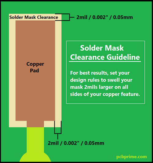
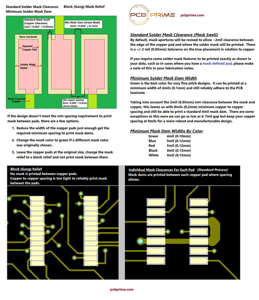
We recommend a 2mil (0.05mm) swell on all sides. If your design rules are set much larger or smaller than this, we will automatically adjust the swell to be around 2mil.
As a general rule, we will resize mask clearances to be approximately 2mils larger on each side of the copper feature to ensure it isn't partially covered with mask. As with everything else, there is a tolerance on the exact placement of the mask on a PCB. The tolerance for mask placement is ± 2mils (±0.05mm) of its intended true position. Even if mask alignment is shifted by the full 2mil tolerance, your entire copper pad should be still solderable.
- TIP: If you are intentionally making your mask clearance smaller than the copper feature it's exposing; this is called a Solder Mask Defined pad (SMD). This is ok to do but please let us know this is your intent, otherwise the order may go on engineering hold or it may be automatically resized per our standard tooling process to be larger than the copper feature.
Solder Mask Defined Pads (SMD)
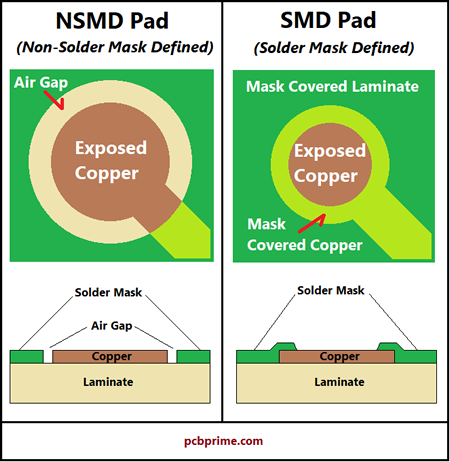 A Non-Solder Mask Defined (NSMD) pad is a traditional solder mask clearance that's larger than the copper pad it's exposing. Most solder mask apertures are NSMD. The mask clearance will be approximately 1.5mil-2mils (0.038mm - 0.05mm) larger than the copper feature on all sides to ensure no mask is accidentally printed on the copper. This is to prevent mask from accidentally being applied over the copper surface, thereby reducing the solderable surface area making soldering more difficult.
A Solder Mask Defined (SMD) pad has a solder mask clearance that is smaller than the copper feature and mask is intentionally printed over a portion of the copper. This is typically only seen on very tightly spaced footprints like BGAs where there simply isn't enough room to print a NSMD with the appropriate clearances.
When designing a solder mask defined pad, make your copper pads as large as you can so a complete copper pad will be exposed in the mask. There is a tolerance on the actual mask placement, so if the mask is only slightly smaller than the pad, there's a chance the mask could shift enough exposing bare laminate which would result in even less solderable surface area. A good rule of thumb is to have a large enough copper pad that will allow you to print at least 3mils (0.076mm) of mask on all sides of your copper pad.
Should I Put Solder Mask Between All Surface Mount Pads?
The short answer is yes, put them between as many pads as you can and cover as much of the board as you can. Mask dams will increase the likelihood the solder will remain in the desired location and you'll have a stronger solder joint. When solder reflows, it liquefies and can easily run, resulting in solder starvation. Symptoms of solder starvation are:
 Intermittent Connection
- Intermittent Shorts
- Poor Solder Joint Strength
- Increased Inspection Time
- Increased Rework
- Higher RMA Costs for Field Failures
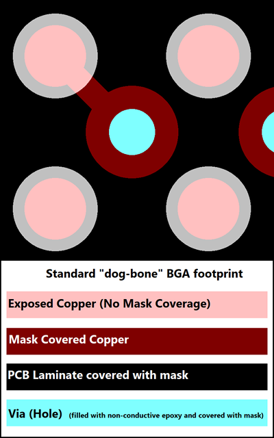
Traditional "dog-bone" pattern BGAs (ball grid arrays) are especially prone to solder starvation due to the proximity of open vias close to the footprint of the chip. We always recommend filling those vias that are underneath or very close to BGAs, with a non-conductive epoxy and applying solder mask over the top of the hole to prevent solder run off.
Other techniques used to handle this issue are the use of Via In Pad (a.k.a. Active Pad) and Solder Mask Defined Pads, confusingly sometimes abbreviated SMD.
More information on Via In Pad can be found in our article on Different Via Types on a PCB
Download a copy of Solder Mask - Min Mask Dam - Min Mask Clearance - Mask Gang Relief.pdf
If you have any questions, please contact us; we will be glad to assist you with your array!