PCB-TIPS
Accepted File Formats
Array Design
CAM Tooling Guidelines
Controlled Dielectric or Controlled Impedance?
Countersink vs Counterbore
Default Rigid PCB Specs
Dielectric Stacks
Drilling and Drill File
Fabrication Drawing/Fab Print
Fabrication Process
Final Finish Comparison
How Thick Is 1oz Copper?
How to Avoid Engineering CAM Hold
Minimizing Bow and Twist
Solder Mask
Via Tenting, Plugging, and Filling
What is Copper Thieving?
How Thick Is 1oz Copper?
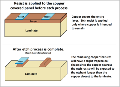
In the printed circuit board industry, the most common way to express copper thickness on a PCB is in ounces (oz). Why use a unit of weight to specify a thickness? Great question! If 1oz (28.35 grams) of copper is flattened to evenly cover 1 square foot of surface area (0.093 square meter), the resulting thickness will be 1.37mils (0.0348mm). A conversion chart for different units of measure can be found below.
Copper Thickness Conversion Chart
| oz | 1 | 1.5 | 2 | 3 | 4 | 5 | 6 | 7 | 8 | 9 |
| mils | 1.37 | 2.06 | 2.74 | 4.11 | 5.48 | 6.85 | 8.22 | 9.59 | 10.96 | 12.33 |
| inch | 0.00137 | 0.00206 | 0.00274 | 0.00411 | 0.00548 | 0.00685 | 0.00822 | 0.00959 | 0.01096 | 0.01233 |
| mm | 0.0348 | 0.0522 | 0.0696 | 0.1044 | 0.1392 | 0.1740 | 0.2088 | 0.2436 | 0.2784 | 0.3132 |
| µm | 34.80 | 52.20 | 69.60 | 104.39 | 139.19 | 173.99 | 208.79 | 243.59 | 278.38 | 313.18 |
How much Copper do I need?
By a wide margin, most PCBs are made with 1oz copper on each layer. If your files do not include a fab print or other specifications, we'll assume 1oz finished copper weight on all copper layers. If your design requires higher voltages, resistance, or impedances, thicker copper might be necessary. There are several online tools that can help you determine what thickness, width or length your traces need to be to achieve your target results. A few such 3rd party tools are linked below. PCB Prime is not affiliated with the authors of these tools.
https://www.eeweb.com/tools/microstrip-impedance
https://www.allaboutcircuits.com/tools/
TIP: Every copper layer is assumed to have the same finished copper weight unless otherwise specified in your fabrication notes. A 4-layer board with a defined weight of 1oz, is assumed to have a finished copper thickness of 1.37mils (or more) on every copper layer.
Copper Weight Minimum Spacing Rules
The thicker your copper requirements are, the more spacing is required between copper features on your PCB.
Cu |
Min. Recommended |
1oz |
3.5 mil (0.089mm) |
2oz |
8 mil (0.203mm) |
3oz |
10 mil (0.254mm) |
4oz |
14 mil (0.355mm) |
TIP: The spacing shown in this chart is to be used as a general guide. Different factories will have slightly different capabilities. This should give you a general idea of what min spacing and min trace width to target when setting your design rules. The more spacing you can give between copper features the better.
It is easier to print narrow traces than it is to etch a narrow gap between them, but for consistency, use the same dimensions for spacing and trace widths for your design rules.
Copper Distribution should be as even as possible
 As a general rule, copper should be distributed as evenly as possible throughout your design. Not only in regard to the copper thickness on each layer, but also how it's distributed across the layer. Of course, this isn't always possible, but keep this in mind during layout.
Plating and etching are organic processes in the sense that the copper clad laminate is submerged into a vat of chemicals for processing. There isn't precise control over where the copper is removed from or plated onto. During etch, the intended image is masked off to protect it from the etchant, but the chemicals in the tank dissolve the copper at slightly different rates depending on where the features are on the panel, the panel's placement within the tank itself, and how densely or sparsely the copper features are distributed.
The chemical solution in the plating and etching tanks are agitated and circulated during processing to minimize these inconsistencies; however, a panel with drastically different copper densities can prove problematic. During your design phase, try to evenly distribute your copper across the entire board rather than having large open spaces with isolated features.
Can I have more copper on one layer than another?
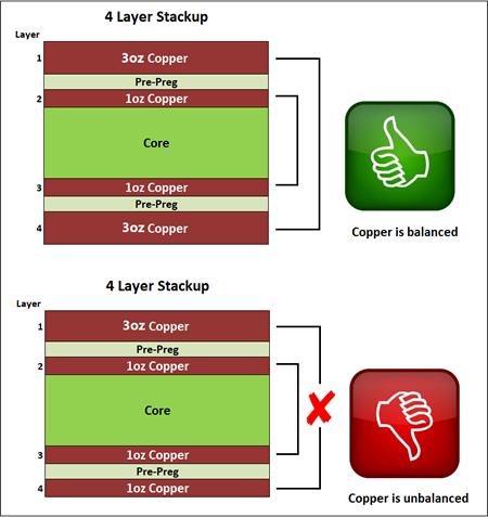 Yes. It's common for there to be heavier copper on some layers than others, for example having 3oz copper on outer layers but 1oz copper on the inner layers, or vice versa. Best design rule practice calls for the same copper weight to be used on the mirror opposite layer in the stack up. Take a 4-layer board for example: layers 1 and 4 can be 2oz and layers 2 and 3 can be 1oz. This gives a balanced stack, reducing the chance the board will bow or twist when heated during use or under the high temperatures used during assembly.
Outer layers should always have the same copper weight.
For example, if the top copper layer is to have a finished copper weight of 2oz, then the bottom layer should also be 2oz. If a different copper weight is specified for top and bottom, say 2oz on top and 1oz on bottom, then the amount of time required to etch through the top side copper will be longer than needed for the bottom. This would result in over etching the bottom layer. Each side would have to be processed independently adding complexity and time to the process. Many factories will not attempt this so avoid this unless necessary. Not only will it add cost, and reduce the number of factories capable of manufacturing the board, but it will also increase the likelihood your board will bow or twist.
Click for more information about copper distribution and thieving.