PCB-TIPS
Accepted File Formats
Array Design
CAM Tooling Guidelines
Controlled Dielectric or Controlled Impedance?
Countersink vs Counterbore
Default Rigid PCB Specs
Dielectric Stacks
Drilling and Drill File
Fabrication Drawing/Fab Print
Fabrication Process
Final Finish Comparison
How Thick Is 1oz Copper?
How to Avoid Engineering CAM Hold
Minimizing Bow and Twist
Solder Mask
Via Tenting, Plugging, and Filling
What is Copper Thieving?
How to Avoid Engineering CAM Hold – PCB Fabrication
Below are common omissions and errors that we routinely find when reviewing printed circuit board design files for fabrication. Before a PCB can begin the manufacturing process, a CAM engineer must review the data submitted and make sure all necessary files are present, there are no questions regarding how the board should be built and also confirm the design can be manufactured as designed.
Ideally, only files that pertain to the bare PCB fabrication will be included in the zip. Extra files submitted will be ignored but it takes time to evaluate these files and determine if they are relevant to the bare PCB fabrication process so please eliminate any irrelevant or duplicate files from your zip.
- Send all necessary files in a single .zip or .rar file
- Separate file for each copper layer in your design.
- Separate file for each top and bottom solder mask (if required).
- Separate file for each top and bottom silk screen (if required).
- Board Outline. Make sure at least 1 of your layers contains a board outline so we know where the true edge of your PCB is. The outline may be placed on any layer and the line can be any thickness you choose, the most common thickness we see is 10mil. Because the thickness of the line is up to you, we assume the middle of the line is the true board edge rather than the inside or outside edge of the line.
- TIP: Although you can place the outline on any layer, it's highly recommended to have a dedicated layer for only the CNC routing lines. This way if there are any internal cutouts or slots in your board, they are not missed because it looks like a line in silk screen, solder mask or copper.
- CNC Drill File. This is the most frequently missed file since many layout programs require a second step to generate this file. The file should be in Excellon Format, ASCII Odd/ None, 2.4 Trailing Zero Suppression, English Units, No Step and Repeats.
- Tool List. A tool list is sometimes used in conjunction with the drill file. The drill file shows where the drills are located and the tool list tells us what size the drills (tools) are and if they should be plated or non-plated. Some layout programs combine the drill file and tool list into the same file but others generate 2 separate files. (Common extensions for this file are: .tol and .rep).
- Fab Print. This can be combined with one of the other layers or on its own dedicated layer. A fab print layer should contain all specifications related to how the bare printed circuit board should be manufactured. A non-Gerber file can be used for your fab print, common file types are: txt, doc, docx, PDF and DXF.
- TIP: Please don't send more information than is required to manufacture your board. We've seen some zip file packages that contain an entire project directory structure within them with many nested sub folders and loads of extraneous or duplicate information.
- Fab Print (Fabrication Print)
- A fab print is not required but it is helpful. A good fab print will outline all the specifications your design requires and could potentially avoid unnecessarily holding up your order for clarification during the engineering process. The print can be on a separate Gerber layer or in a readme.txt, PDF or .doc(x). An example fab print is shown below.
- Material Type (ex: FR4, High Tg FR4, Rogers 4350..etc)
- Finished Thickness of the board
- Finished Plating (ex: Lead Solder, Immersion Gold..etc)
- Finished Copper Weight of each copper layer. Typically expressed in ounces. (ex: 1oz, 2oz)
- Solder Mask Color
- Silk Screen Color
- Dimensions of the board
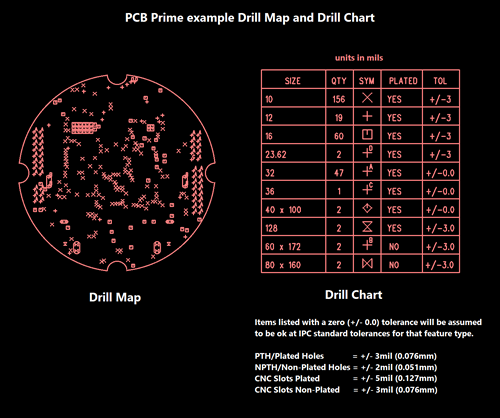
- Drill Chart showing:
- Quantity of each hole size on the board
- Whether the holes are plated or non-plated
- Size tolerance (IPC Standard is +/- 3mil for plated holes, +/- 2mil for non-plated holes)
- Slot size and whether they are plated or non-plated
- Any other notes our engineering team needs to be made aware of
Read our tip on Fabrication Drawings for more detail
If your files don't call out a specification, we will assume the following standards.
PCB Prime Rigid PCB Default Specifications Finished Board Thickness 0.062" (1.6mm) Material Type RoHS Compliant 135°Tg FR4 Final Plating Finish Lead Free Solder (LF HASL) Copper Weight (Thickness) 1oz / 0.00137" / 1.37mil /0.035mm - All Layers Finished Cu Thickness Solder Mask Color Green – Both sides of the board Silk Screen Color White – Applied to sides where silk screen files are provided Build and Inspection Class II / IPC-600A / IPC-6012 latest revisions ITAR Not ITAR Compliant UL Markings No UL or other markings will be applied unless requested RoHS Compliant Yes REACH Compliant Yes Conflict Free Materials Yes Electrical Test Yes
Read our article on Default Rigid PCB Specs
- A fab print is not required but it is helpful. A good fab print will outline all the specifications your design requires and could potentially avoid unnecessarily holding up your order for clarification during the engineering process. The print can be on a separate Gerber layer or in a readme.txt, PDF or .doc(x). An example fab print is shown below.
- Send your design files in the correct format
Gerber 274X: We prefer to receive files in 274X Gerber format, this is the most current Gerber format and all modern PCB layout tools will output in this format. This format has the apertures embedded within the files so a separate aperture file is not required. We also accept the legacy 274D Gerber format.
Gerber 274D: We can accept files in older 274D Gerber format where the apertures are in a separate file.
ODB++: We also accept ODB++ files. If we received a file package containing Gerber and ODB++ files, we will defer to the Gerber file set to manufacture from.
CNC Drill File: Along with your Gerber file, we also need a Drill File in the following format. Excellon Format, ASCII Odd/ None, 2.4 Trailing Zero Suppression, English Units, No Step and Repeats. This file is used to program the CNC drill machine. ODB++ files will typically include the CNC drill file in the directory structure.
Tool List: Many software packages combine this file into the drill file but some create separate files for this. (Common extensions for this file are: .tol and .rep).
DXF: In some cases, we can also convert DXF files into 274X Gerber files. We will review these on a case by case basis.
Only have a picture or physical board? Unfortunately, we cannot manufacture a PCB from a picture, PDF, or a physical board. We need digital files in one of the file formats mentioned above. If you have a board in hand that you'd like to get a more copies of, this would need to be scanned, reverse engineered, and digital files created before we could manufacture it. There are several companies that do this type of service, we recommend searching for PCB Reverse Engineering Services. Once you have the digital files, we will be happy to help you manufacture your project.
- Missing Solder Mask Clearances
We will do our best to do a 'reality check' on the placement of your solder mask clearances. We will review where they are or are not found. We will question areas we find that appear as if a mask clearance is either missing or extraneous.
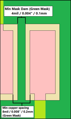 Copper Spacing is too tight to allow solder mask to be printed between pads
There is a limit to how narrow a 'mask dam' can be printed and reliably adhere to the PCB laminate. Different mask colors and copper weights require a thicker or thinner min width for a solder mask dam.
For more information on this topic, read our article on Solder Mask or refer to Solder Mask - Min Mask Dam - Min Mask Clearance - Mask Gang Relief.pdf
- Copper Trace Width/Trace Space is too tight to manufacture
Trace width = The width of the copper feature
Trace space = The distance between 2 copper features sometimes referred to as the 'air gap'.Refer to the chart below for guidelines on how to set your design rules based on your finished copper weight.
Cu
WeightMin. Recommended
Space between
Copper Features
and Min. Trace width1oz
3.5 mil (0.089mm)
2oz
8 mil (0.203mm)
3oz
10 mil (0.254mm)
4oz
14 mil (0.355mm)
- TIP: The spacing shown in this chart is to be used as a general guide. Different factories will have slightly different capabilities. This should give you a general idea of what min spacing and min trace width to target when setting your design rules. The more spacing you can give between copper features the better.
It is easier to print narrow traces than it is to etch a narrow gap between them, but for consistency, use the same dimensions for spacing and trace widths for your design rules.
- TIP: The spacing shown in this chart is to be used as a general guide. Different factories will have slightly different capabilities. This should give you a general idea of what min spacing and min trace width to target when setting your design rules. The more spacing you can give between copper features the better.
- Conflicting specifications ordered online vs what is detailed in the fab print
Make sure the specs ordered online match the specs in your fab or we'll have to hold the order to figure out which is correct. It's ok to order a different specification than what your files state, but please make a note of this on your order or let your account representative know so we can avoid an engineering hold.
- Conflicting specifications between the fabrication drawing and Gerber
We will review the fabrication drawing to make sure the dimensions, hole count and locations, etcetera match what we see in the digital layout files. If we find a discrepancy, we will hold the order to confirm which is correct.
 Missing or Conflicting Drill Information
We compare the CNC Drill file to the fabrication drawing. Be sure to update the fab print with any changes to the number of drills, sizes, locations, and properties such as plated or non-plated. Discrepancies can easily occur when up revving a board and a revised fab print isn't created.
Also make sure to include a drill chart so we know which holes should be plated (PTH) or non-plated (NPTH). By default, we will assume all holes should be plated. For the electroplating process to work in a hole/via, there needs to be a copper pad surrounding the hole on the 2 outside layers. (Annular Ring).
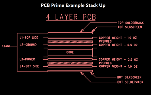 Missing Layer Stack Up (Layer Order)
On multilayer boards, 4 copper layers or more, make sure to include information for what order the inner layers should be arranged. This can be conveyed by stating the layer number in the file name, a fab print containing a stack up chart cross referencing the copper layer files to the correct position or even a simple readme.txt stating the correct order. As long as we have some way to determine the correct stack order we won't need to ask.
- Copper Too Close to Board Outline or Cutout
If copper is too close to the outline or cutout, the copper could become damaged by the router bit or score blade and may be exposed along that edge. As a general rule, here are the recommended minimum clearances.
CNC Route Outer Layer Copper<.td> = 10 mils from center of route line. Inner Layer Copper = 10 mils from center of route line. Scoring (Board Thickness 0.062" thickness / 1.6mm) Outer Layer Copper = 15mils from center of score line Inner Layer Copper = 20 miles from center of score line TIP: Thicker scored boards require more clearance. 0.093" boards for example will require an extra 5mils of clearance when scoring. - Missing or Incomplete Controlled Impedance Information
Make sure any controlled impedance lines can be easily located so we know which lines are to be controlled. The best way to do this is to make these lines a unique width from any other traces on the board. This way we can search for all 6.5mil wide D-Codes for example. Referring to a net name is generally not helpful.
If you can't make the lines a unique width, then a simple picture with the intended traces circled or highlighted will also work.
- Controlled Impedance Adjustments
We build a lot of boards with controlled impedance requirements. Our CAM engineers will run the board characteristics through Polar modeling software to calculate the best way to accurately reach your target impedance. It's rare to receive files for a controlled impedance PCB were the trace widths, copper to copper spacing, and dielectric spacing between layers is already 100% accurate and no fine tuning is required.
If your design requires controlled impedance and you supply recommended trace/widths and dielectric spacing, please also add a note that we may adjust the design as needed to reach the target impedance. Otherwise, we may need to hold the order to get your approval to make the necessary adjustments. Of course, if you'd like to approve of any changes, we can hold the order after CAM is complete so you can review. The production clock won't begin until the files are approved and we can begin manufacturing.
If you have any questions, please contact us; we will be glad to assist you with your array!