PCB-TIPS
Accepted File Formats
Array Design
CAM Tooling Guidelines
Controlled Dielectric or Controlled Impedance?
Countersink vs Counterbore
Default Rigid PCB Specs
Dielectric Stacks
Drilling and Drill File
Fabrication Drawing/Fab Print
Fabrication Process
Final Finish Comparison
How Thick Is 1oz Copper?
How to Avoid Engineering CAM Hold
Minimizing Bow and Twist
Solder Mask
Via Tenting, Plugging, and Filling
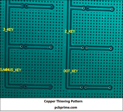
What is Copper Thieving?
What is Copper Thieving?
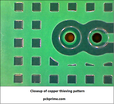 Copper Thieving is just a fancy way of saying that small copper circles, squares or even a solid copper plane will be added to larger blank spaces to even out the copper distribution across a copper layer. The added copper isn't connected to any nets on the board and should not affect the functionality. Care will be taken to ensure thieving will not interfere with any defined controlled impedance or RF signal lines the design may contain. If you have specific RF or impedance requirements that thieving may impact, please add a fabrication note that copper thieving is not permitted or should be avoided in certain areas.
Why would a board shop add copper thieving to my design?
Etching and Plating Control
 There are many reasons copper thieving may be added to a PCB. The primary reason is to make the copper distribution across a layer as uniform as possible to make etching and plating more predictable. The etch and plating processes are performed by submerging a copper clad panel into a chemical bath, so areas that have different copper densities will plate and etch at different rates. For example, a small copper feature, with relatively no copper adjacent to it, will be prone to both over etching and over plating. This could result in an unpredictable size for this feature.
Most of the additional plating a PCB receives is through an electrolytic plating process which passes electrical current through the production panel. Copper features such as traces, pads, and plated vias, that are in a more sparsely populated area, will tend to over plate compared to those in more densely packed areas where the electrical current is distributed among other features.
Consistent Finished Thickness
Another reason to add thieving is to even out the finished thickness of the board. If your design has 8 copper layers and most of the copper is stacked on the left side of each layer, there could be a noticeable change in board thickness from one side to the other. The thickness of 1oz of copper is 1.37mil (0.035mm), so you can see how quickly the stacked areas of copper vs no copper could result in a different finished thickness.
Minimize Bow and Twist
In some cases, uneven copper distribution could result in the PCB warping or twisting, especially during high assembly or usage temperatures when the copper begins to heat and expand. A great example of this is the Eiffel Tower. It's 6.75" (17cm) taller on a hot summer day than it is at night.
Control Dielectric Thickness Between Layers
Thieving may be added to more accurately control the dielectric thickness between copper layers. Think of pre-preg as the glue that bonds the layers together. Pre-preg stands for "Pre-Impregnated". It's a flexible fiberglass-based material that has been impregnated with a semi-cured epoxy resin. It looks and feels like thick wax paper. During the lamination cycle, the layers are stacked together, with sheets of pre-preg between them. The lamination book is heated and pressed. The pre-preg will liquefy and flow to fill in the gaps between the copper features to ensure no air is trapped inside the board. Trapped air would heat up during assembly, potentially outgassing causing delamination or even ejecting components off the board. If the copper distribution is uneven, it will be more difficult to control how much pre-preg to use which may result in inconsistent dielectric thicknesses.
Reduce Cost Due To Excessive Etch
Each copper layer in a PCB begins the process as a solid copper sheet. To reveal the copper pattern, the excess copper needs to be etched away. The etched copper is suspended in the etching solution. There is a limit to how much copper can be etched by the chemical solution before the solution becomes over saturated with copper and becomes ineffective. Once the saturation point is reached, the tank must be drained, and fresh chemicals added.