PCB-TIPS
Accepted File Formats
Array Design
CAM Tooling Guidelines
Controlled Dielectric or Controlled Impedance?
Countersink vs Counterbore
Default Rigid PCB Specs
Dielectric Stacks
Drilling and Drill File
Fabrication Drawing/Fab Print
Fabrication Process
Final Finish Comparison
How Thick Is 1oz Copper?
How to Avoid Engineering CAM Hold
Minimizing Bow and Twist
Solder Mask
Via Tenting, Plugging, and Filling
What is Copper Thieving?
PCB Fabrication Process
There are many steps to manufacturing a printed circuit board. Below is a brief overview of the manufacturing process of a standard 4-layer board. For simplicity sake, the steps below are a condensed version of the processing required. Some standard processes such as cleaning, rinsing, pre-treating, baking, were omitted from the workflow.
There are many additional steps that could be included in the workflow depending on the requirements of the design. Higher technology boards may require multiple drill and lamination cycles for blind and buried vias (HDI) construction. Impedance calculations, adjustments and testing, via in pad (VIP/Active Pad) processing, countersinks, counterbores, gold fingers… the list goes on.
Step 1: CAM/Setup/Tooling
The first step to manufacturing your design is to review all submitted files, align the layers and make adjustments for production. At PCB Prime, a full DFM (Design For Manufacturing) review is performed to ensure the board is manufacturable as designed. If any problems or questions are found, we will hold the order and contact you for clarification. A more detailed explanation of the CAM process can be found at our CAM Tooling Guidelines tips page.
Click this link if you would like tips on How to Avoid Engineering CAM Hold
Step 2: Select Materials
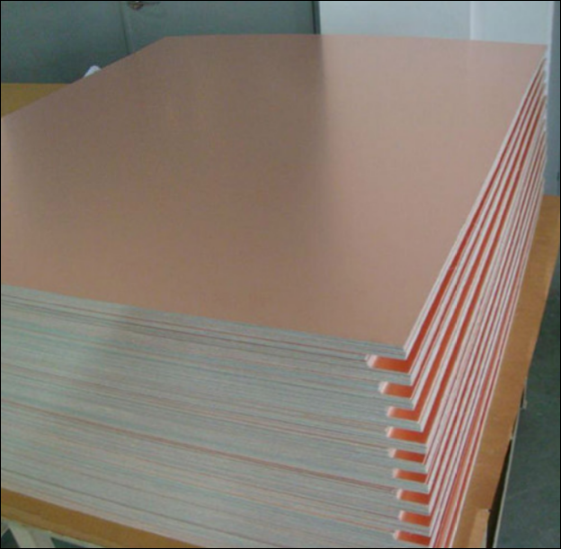
 We stock a variety of different thicknesses and brands of pre-fabricated cores and pre-preg materials to meet the many different dielectric thicknesses and copper weights we build. When making a 4-layer board, the center core is processed first. The center core in this example comprises layers 2-3.
Step 3: Imaging
 Cores arrive at our factory from the laminate suppliers pre-clad with copper on both sides. The excess copper needs to be chemically etched away, leaving only your intended copper features on the board.
To do this, the entire panel is covered with a UV sensitive etch resist. This resist is then exposed to a high intensity UV lamp to cure and bond it to the copper surface. The UV light passes through a film containing a photo plotted image of your copper pattern derived from your Gerber file. The photo plotted pattern is a negative image of your design. This means where you intend for there to be copper, the film is clear allowing the UV light to pass through, cure and bond the etch resist to the copper. Where copper needs to be removed, the film is black, preventing the resist from bonding to the copper, allowing it to be washed off before the etch process.
TIP: A standard 2-layer board will skip steps 3, 4, 5, 6.
Step 4: Etching
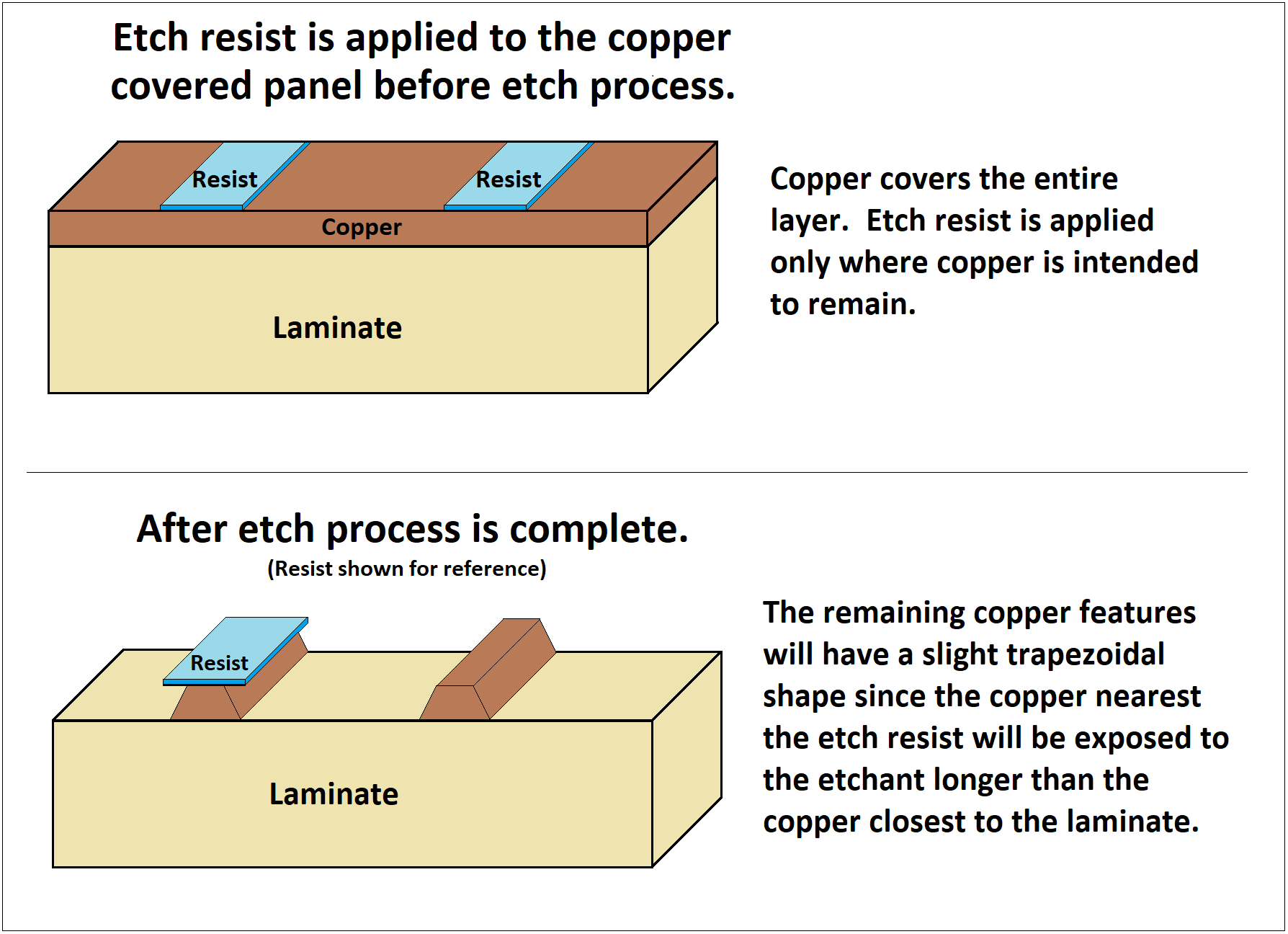 The panel is now submerged in a chemical bath to remove the excess copper not protected by the resist in step 3. Since the resist can only be applied to the surface of the copper, the etchant will begin removing copper in all directions. It will etch laterally underneath the resist as well as down towards the laminate. Since this is a chemical process, the resulting shape of a trace or pad with be slightly trapezoidal. Thicker copper will require more time to etch, which will exaggerate the shaping of the features.
To compensate for this lateral etching underneath the etch resist, your copper features are enlarged slightly during the CAM Tooling process. The thicker the copper is, the more compensation is needed to ensure your copper features are the correct size after processing. Because of this, heavier copper weights require more space between copper features.
More information can be found in our How Thick Is 1oz Copper? PCB Tip.
Step 5: AOI (Automated Optical Inspection)
 Inner layer cores are now examined by AOI equipment to ensure proper etching and ensuring there are no opens or shorts.
Step 6: Lamination
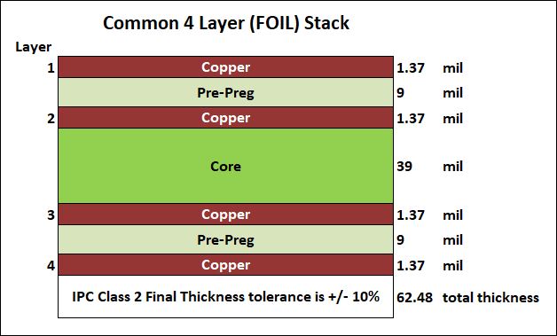
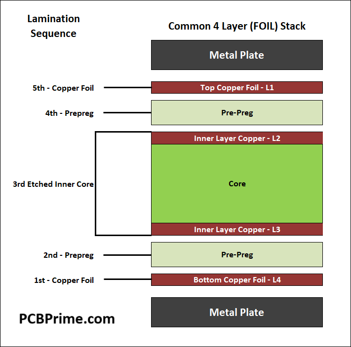 The inner layers are now ready to be bonded with the outer layers. The stack is built from the bottom up so the bottom side copper foil is placed into a fixture consisting of a metal plate containing mounting pins that correspond to the pre-drilled tooling holes in the materials being used. This ensures proper alignment between the layers. An example of a 4-layer stack sequence is shown below in order of placement in the lamination book.
-
5. Top Layer Copper Foil
4. Prepreg
3. Etched Inner Layer Core
2. Prepreg
1. Bottom Layer Copper Foil
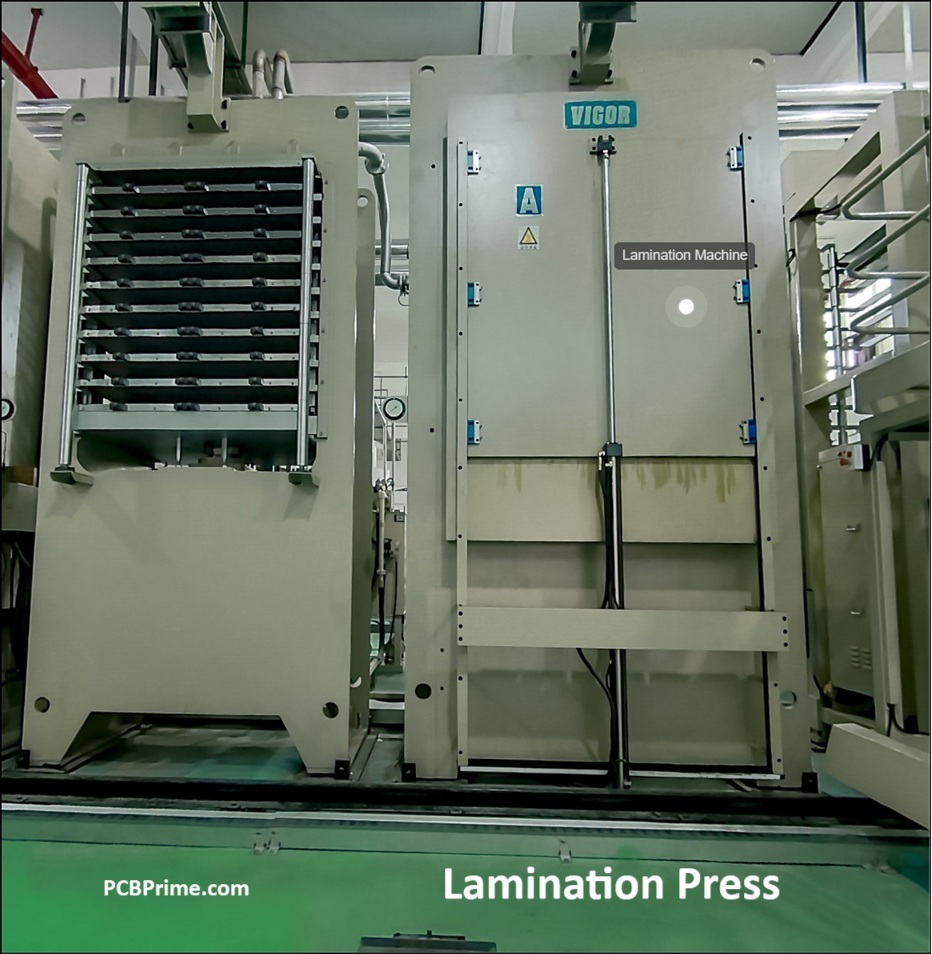 After the top foil is affixed to the stack, a heavy metal plate is placed on top. The process can be repeated so multiple panels can be stacked within the same book allowing several panels to be processed at the same time. When the entire sequence is complete, it's placed into a heated lamination press so the prepreg can liquefy and flow into the gaps which are caused by the height difference between the areas of copper and bare laminate on the inner cores. The total copper area on each layer is pre-calculated at the CAM/Tooling step, so the lamination department knows how much prepreg is needed to ensure all gaps are filled and the correct final dielectric thickness between copper layers is met.
Step 7: Drill (Primary PTH)
 Now that all the layers have been bonded together, we are ready to perform the primary drill. Only holes that require copper plating in the barrels are usually drilled at this step. PTH stands for (Plated Thru Hole). Any non-plated (NPTH) holes are usually drilled at the final CNC routing step but it is possible to drill both PTH and NPTH at this step.
Just like the lamination step where several panels are stacked on top of each other to expedite processing, the same is typically done at drill. Multiple panels are stacked on top of each other so 2-3 panels can be drilled simultaneously with a single drilling head.
Step 8: Deburr and Desmear
Just like when drilling into wood, drilling into fiberglass causes debris and burrs to be left in and around the edges of the holes. A mechanical deburring process is performed to remove any unwanted material to provide the cleanest possible surface for the plating process in the next step. This is a combination of compressed air, light brushing, and high-pressure water rinse.
Drill bits get hot when drilling through laminate and copper, especially when spinning at up to 150,000 RPM on smaller size bits. This friction can cause resin in the laminate to become hot enough to reflow the resin in the laminate, leaving a thin film coating the hole walls. The desmear process is a chemical solution, either permanganate or plasma etch, that is used to remove any unwanted remaining resin.
Step 9: Outer Layer Copper Plating
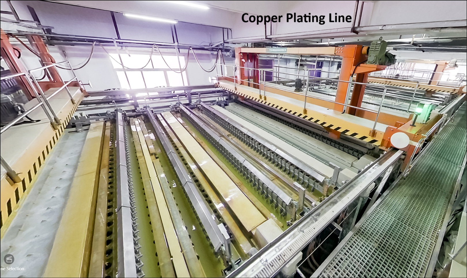 Now it's time to get copper plating into the barrels of the through holes and plate up the outer surface layers with the final deposition of copper to reach the desired copper final thickness. As mentioned previously, if your design requires a 1oz finished copper weight, we will use raw material that's pre-clad with 1/2oz copper on each side. The additional 1/2oz will be added to the surface during the plating process. Usually a little more than 1/2oz copper is plated at this step to ensure enough copper is deposited in the plated thru holes (PTH).
More information can be found in our How Thick Is 1oz Copper? PCB Tip.
TIP: Since inner layers are already laminated together at this stage, they will not receive additional plating, aside from the plating that lines the hole walls. Inner layer cores begin with their target copper thickness.
 Electroplated copper won't bond directly to the hole walls. First, a chemical plating process is used to deposit a very fine layer of copper onto the hole walls. (Electroless Copper Deposition) After the hole wall surface is completely covered with copper, the rest of the required copper can be deposited using a standard electrolytic plating process. During the electrolytic process, the entire production panel is suspended from a buss bar and submerged into a plating tank. The buss bar passes electrical current though the panel which draws copper atoms out of the plating solution and bonds them to the copper already present on the panel.
TIP: IPC Class 2 specification for min average plating thickness of a plated hole is 0.79mil (20µm/787µin).
Step 10: Image, Etch and AOI... again?
It was so much fun the first time, let's do it again! At this step, the outer layers are still solid sheets of copper with some plated holes drilled into them, just like the inner layer cores were at step 3. The same image, etch, and AOI inspection process is repeated to reveal the outer layer images and inspected to ensure no opens, shorts or other manufacturing defects.
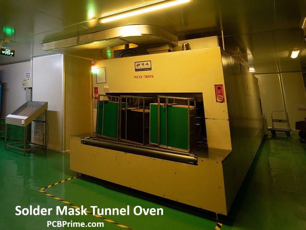
Step 11: Solder Mask
 Now your PCB is starting to come together and is beginning to resemble the final product. Solder mask is what gives your board it's color… usually green but we can use many other colors. For more detail on this step, check out our tips on Solder Mask.
Bare FR4 material is naturally a light yellow/green color.
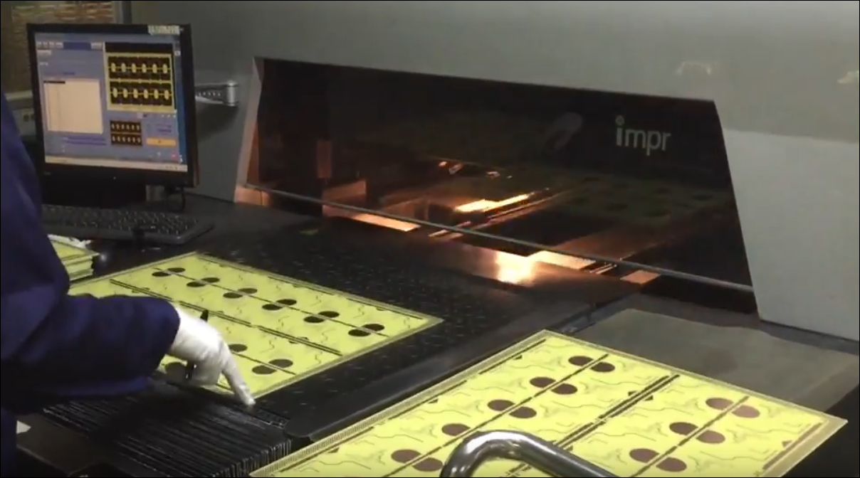
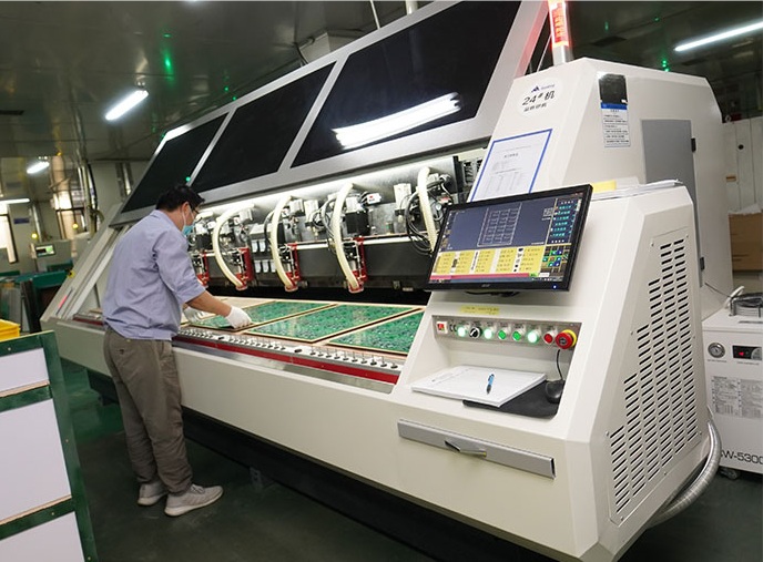
Step 12: Silk Screen
 Now that your board is protected by solder mask, it's time to print the silk screen legend. There are two types of silk-screening processes that are used today. Traditional and ink jet.
The traditional silk screen process requires a mesh screen to be manufactured which allows the epoxy ink to pass through only in the desired places. The screen is placed over the board and ink is squeegeed across the surface of the screen. After the first side is screened, its tact dried long enough to prevent smudging when flipping the panel over and screening the opposite side. Then the panel is placed in an oven to fully cure.
For lower volume orders or where very fine details are required, ink jet processing is the way to go. We have an ink jet style machine that will print just like an ink jet printer.
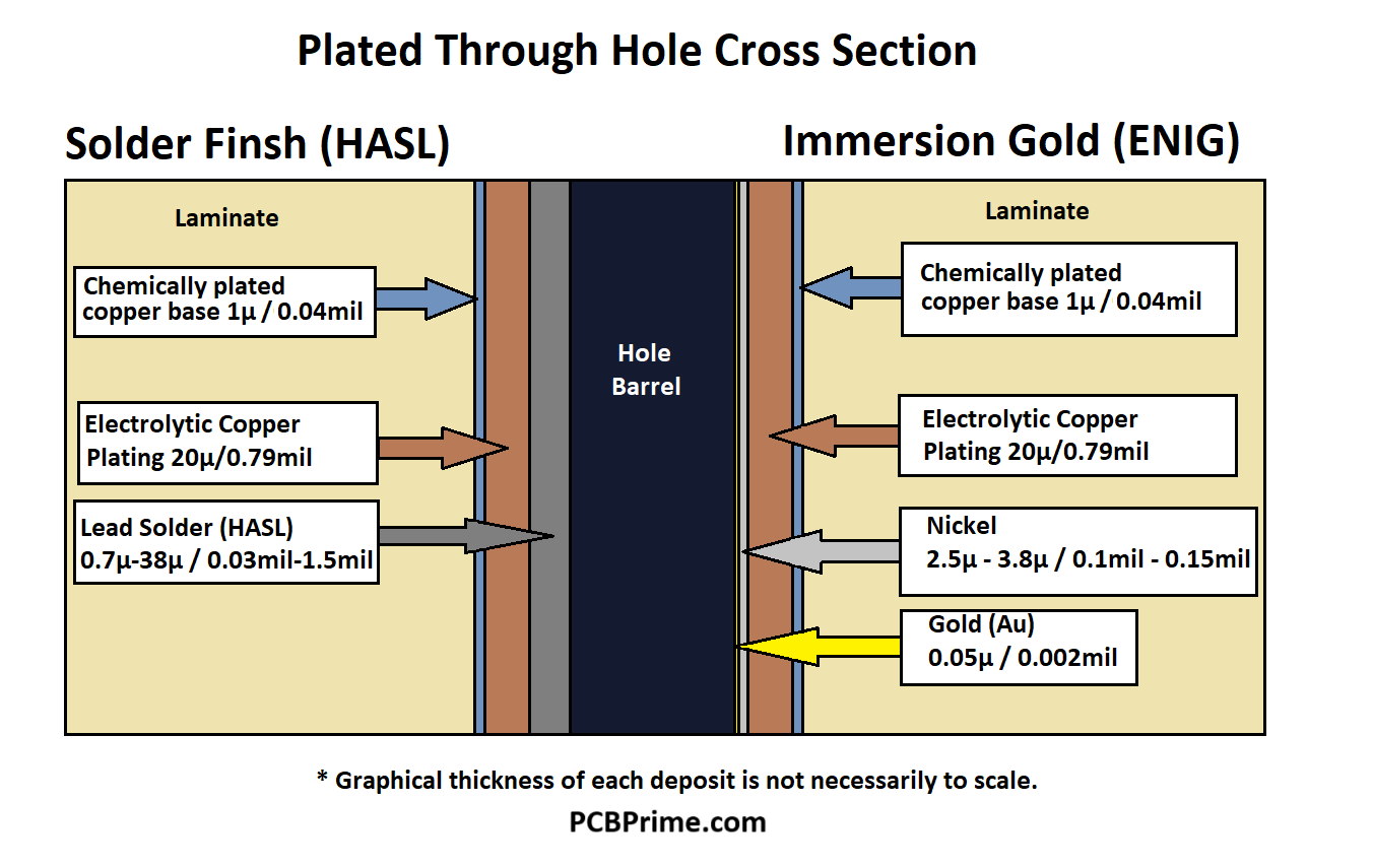
Step 13: Final Finish
At this stage, your board will have a 'final finish' applied to any copper areas that are still exposed to the open air. (Areas not covered by solder mask). The final finish will not only protect the copper from oxidation, but it will also provide a higher quality solderable surface.
In the past, lead solder, also known as hot air solder level (HASL) was the most common finish. Considering today's environmental and health concerns, RoHS finishes such as lead free solder (LF HASL) and immersion gold (ENIG) are much more common than lead solder, although legacy, military or aviation boards may still require lead HASL.
For more in-depth information on final finish options, see our Final Finish Comparison article.
Step 14: Electrical Testing
Even though quality control inspections have been performed at numerous points along the manufacturing process, we will always electrically test your bare board to ensure there are no opens or shorts. At PCB Prime, we never charge extra for this service, we believe the comfort of knowing you've received a quality product should not be an additional expense.
Step 15: CNC Routing and Non-Plated Drill
 Time to route the profile of your design and drill any non-plated thru holes (NPTH). Routing through fiberglass creates a lot of debris so a vacuum is positioned over the routing head to remove unwanted material.
Step 16: Final Quality Control Inspection (FQC)
The boards are again inspected to meet or exceed a minimum of IPC Class 2 requirements. IPC Class 3 is available upon request.
As with any production process, some fall out is expected. If you are ordering boards in a tab-routed or scored array, any boards that are found defective will be marked with a large black 'X' on both sides of the board to indicate they should not be assembled.
We do offer a 'No X-Out' service that guarantees all your arrays will be 100% good boards. It does cost a little more since more arrays need to be manufactured to ensure there are enough 100% good arrays to fill your order. Most assemblers these days have sophisticated assembly equipment and can easily program around X-outs, but we do offer this service if needed. By default, we assume some x-outs are acceptable.
Step 17: Packaging and Shipping
It's time to package the boards in an airtight shrink wrap along with a desiccant pack to extend the shelf life. Your order will be packaged in a box with plenty of padding to ensure they arrive safely and undamaged. You'll receive an automated email with the tracking number of your shipment so you can track your package.
If you have any questions about the manufacturing process or anything else related to PCB manufacturing and assembly, please contact us, we will be glad to help.
PCB Prime